


All Products
Contact Person :
Zhou
Phone Number :
+86 15019457904
Whatsapp :
+8615019457904
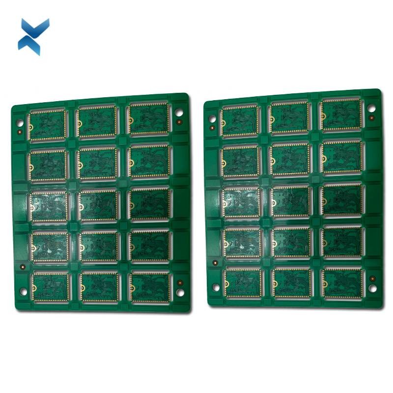
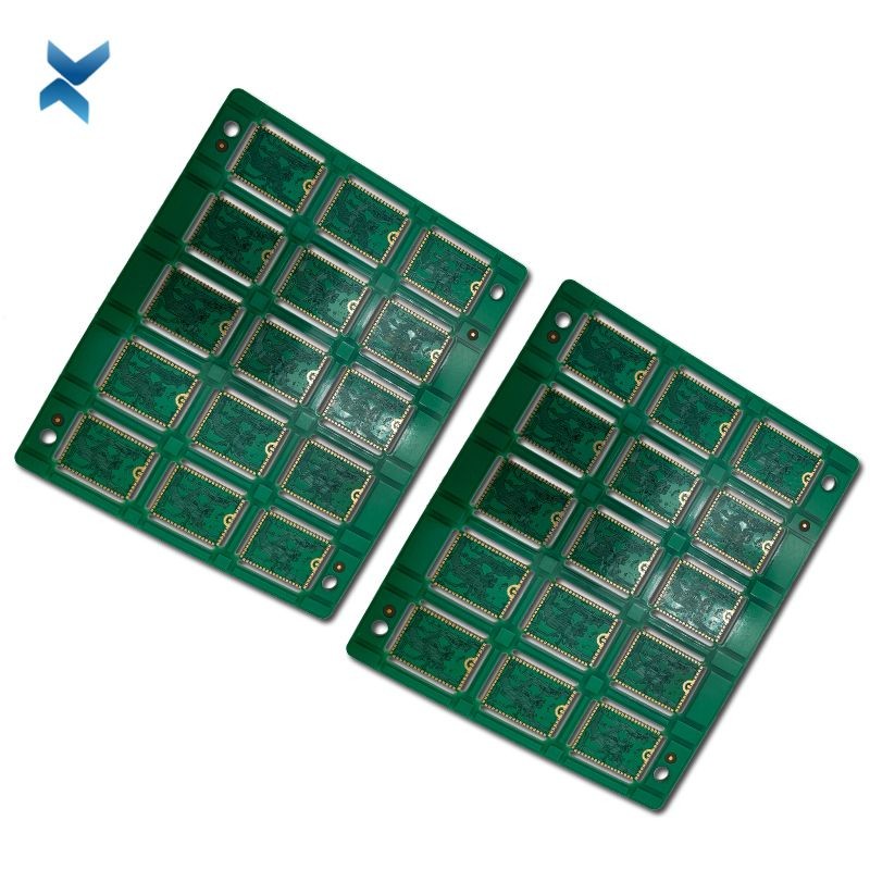
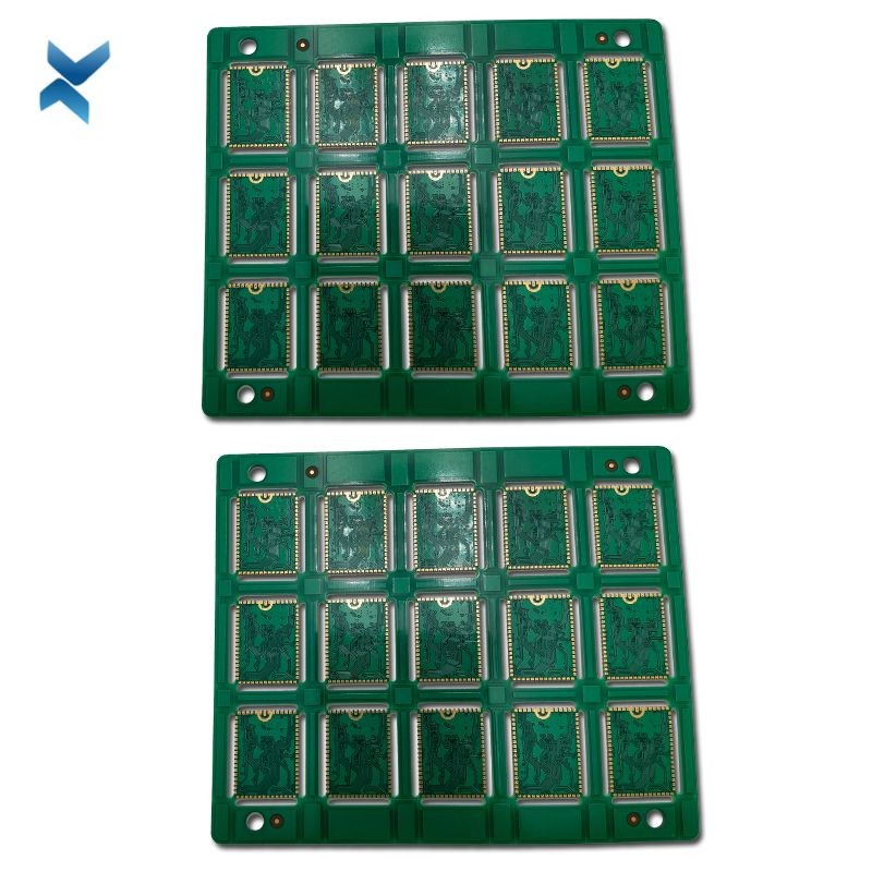
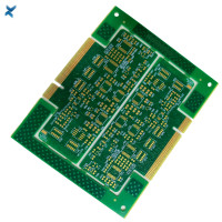
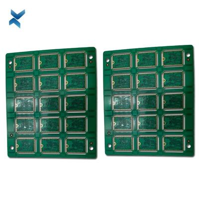
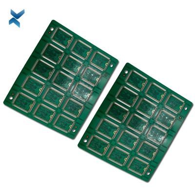
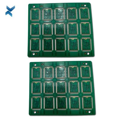
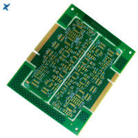
OEM HDI Circuit Boards , PCBA Board Assembly For Consumer Electronics
| Place of Origin | China |
|---|---|
| Brand Name | YS |
| Certification | ISO9001 |
| Model Number | YS-0017 |
| Minimum Order Quantity | 1 |
| Price | 0.2-6$/pieces |
| Delivery Time | 3-8 work days |
| Payment Terms | L/C, T/T, Western Union, MoneyGram |
| Supply Ability | 158000 pieces |

Contact me for free samples and coupons.
Whatsapp:0086 18588475571
Wechat: 0086 18588475571
Skype: sales10@aixton.com
If you have any concern, we provide 24-hour online help.
xProduct Details
| Application | Consumer Electronics | Product Name | Printed Circuit Board |
|---|---|---|---|
| Material | FR4 | Copper Thickness | 0.5oz-8oz |
| Base Material | FR-4 | Min. Line Spacing | 0.1mm |
| High Light | OEM HDI Circuit Boards,PCBA HDI Circuit Boards,Electronics PCBA Board Assembly |
||
Product Description
Please Provide Gerber Bom File Our Factory For You Manufactures OEM Assembly Printed Electronic Circuit Boards PCBA One
What is a HDI PCB?
HDI stands for High Density Interconnector. A circuit board which has a higher wiring density per unit area as opposed to conventional board is called as HDI PCB. HDI PCBs have finer spaces and lines, minor vias and capture pads and higher connection pad density. It is helpful in enhancing electrical performance and reduction in weight and size of the equipment. HDI PCB is the better option for high-layer count and costly laminated boards.
HDI PCB:
High density interconnect PCB, are a way of making more room on your printed circuit board to make them more efficient and allow for faster transmission. It's relatively easy for most enterprising companies that are using printed circuit boards to see how this can benefit them.
Advantages of HDI PCB
The most common reason for using HDI technology is a significant increase in packaging density.
The space obtained by finer track structures is available for components.
Besides, overall space requirements are reduced will result in smaller board sizes and fewer layers.
Usually FPGA or BGA are available with 1mm or less spacing.
HDI technology makes routing and connection easy, especially when routing between pins.
HDI PCB manufacturing methods vary depending on the HDI builds, and the common manufacturing is sequential laminating. The simplest 1+N+1 HDI PCB manufacturing is similar to multilayer PCB manufacturing. For example, a four-layer HDI PCB with a 1+2+1 structure is manufactured in this way:
1. The two inner PCB layers are manufactured and laminated, and the two outer layers are manufactured.
2. The two inner layers are drilled by mechanical drilling. The two outer layers are drilled by laser drilling.
3. Blind vias in the inner layers are electroplated. The two outer layers are laminated with the inner layers.
For the 2+N+2 stacked via HDI PCBs, the common manufacturing method is below (take a 2+4+2 HDI PCB as an example):
1. The 4 inner PCB layers are manufactured and laminated. Layer 2 and layer 7 are manufactured.
2. The inner layers are drilled by mechanical drilling. Layer 2 and layer 7 are drilled by laser drilling.
3. Blind vias in the inner layers are electroplated. Layer 2 and layer 7 are laminated with the inner layers.
4. Microvias in layer 2 and layer 7 are electroplated.
5. Layer 1 and layer 8 are manufactured. The HDI PCB manufacturer locates the places for the microvias and drills by laser drilling.
6. Layer 1 and layer 8 are laminated with the finished PCB layers.
Manufacturing 2+N+2 staggered-via HDI PCBs is easier than 2+N+2 stacked-via HDI PCBs because the microvias do not require high precision for locating and stacking.
In HDI PCB manufacturing, besides sequential laminating, technologies for creating stacked vias and in-hole metallization are also in use. For the higher HDI builds, the stacked vias in the outer layers can also be directly drilled by laser. But direct laser drilling requires extremely high precision for the drilling depth, and the scrap rate is high. So direct laser drilling is seldom applied.
| YScircuit HDI PCB manufacturing capabilities overview | |
| Feature | capabilities |
| Layer Count | 4-60L |
| Available HDI PCB Technology | 1+N+1 |
| 2+N+2 | |
| 3+N+3 | |
| 4+N+4 | |
| 5+N+5 | |
| Any layer | |
| Thickness | 0.3mm-6mm |
| Minimum line Width and Space | 0.05mm/0.05mm(2mil/2mil) |
| BGA PITCH | 0.35mm |
| Min laser Drilled Size | 0.075mm(3nil) |
| Min mechanical Drilled Size | 0.15mm(6mil) |
| Aspect Ratio for laser hole | 0.9:1 |
| Aspect Ratio for through hole | 16:1 |
| Surface Finish | HASL, Lead free HASL,ENIG,Immersion Tin, OSP, Immersion Silver, Gold Finger, Electroplating Hard Gold, Selective OSP,ENEPIG.etc. |
| Via Fill Option | The via is plated and filled with either conductive or non-conductive epoxy then capped and plated over |
| Copper filled, silver filled | |
| Laser via copper plated shut | |
| Registration | ±4mil |
| Solder Mask | Green, Red, Yellow, Blue, White, Black, Purple, Matte Black, Matte green.etc. |
| layer/m² | S<1㎡ | S<3㎡ | S<6㎡ | S<10㎡ | S<13㎡ | S<16㎡ | S<20㎡ | S<30㎡ | S<40㎡ | S<50㎡ | S<65㎡ | S<85㎡ | S<100㎡ |
| 1L | 4wds | 6wds | 7wds | 7wds | 9wds | 9wds | 10wds | 10wds | 10wds | 12wds | 14wds | 15wds | 16wds |
| 2L | 4wds | 6wds | 9wds | 9wds | 11wds | 12wds | 13wds | 13wds | 15wds | 15wds | 15wds | 15wds | 18wds |
| 4L | 6wds | 8wds | 12wds | 12wds | 14wds | 14wds | 14wds | 14wds | 15wds | 20wds | 25wds | 25wds | 28wds |
| 6L | 7wds | 9wds | 13wds | 13wds | 17wds | 18wds | 20wds | 22wds | 24wds | 25wds | 26wds | 28wds | 30wds |
| 8L | 9wds | 12wds | 15wds | 18wds | 20wds | 20wds | 22wds | 24wds | 26wds | 27wds | 28wds | 30wds | 30wds |
| 10L | 10wds | 13wds | 17wds | 18wds | 20wds | 20wds | 22wds | 24wds | 26wds | 27wds | 28wds | 30wds | 30wds |
| 12L | 10wds | 15wds | 17wds | 18wds | 20wds | 20wds | 22wds | 24wds | 26wds | 27wds | 28wds | 30wds | 30wds |
| 14L | 10wds | 16wds | 17wds | 18wds | 20wds | 20wds | 22wds | 24wds | 26wds | 27wds | 28wds | 30wds | 30wds |
| 16L | 10wds | 16wds | 17wds | 18wds | 20wds | 20wds | 22wds | 24wds | 26wds | 27wds | 28wds | 30wds |
30wds |
![]()
![]()
![]()
![]()
![]()
FQA
What is HDI PCBs?
High density interconnect (HDI) PCBs represent one of the fastest-growing segments of the printed circuit board market.
Because of its higher circuitry density, the HDI PCB design can incorporate finer lines and spaces, smaller vias and capture pads, and higher connection pad densities.
A high-density PCB features blind and buried vias and often contains microvias that are .006 in diameter or even less.
1.Multi-step HDI enables the connection between any layers;
2.Cross-layer laser processing can enhance the quality level of multi-step HDI;
3.The combination of HDI and high-frequency materials, metal-based laminates, FPC and other special laminates and processes enable the needs of high density and high frequency, high heat conducting, or 3D assembly.
Recommended Products