


All Products
Contact Person :
Zhou
Phone Number :
+86 15019457904
Whatsapp :
+8615019457904
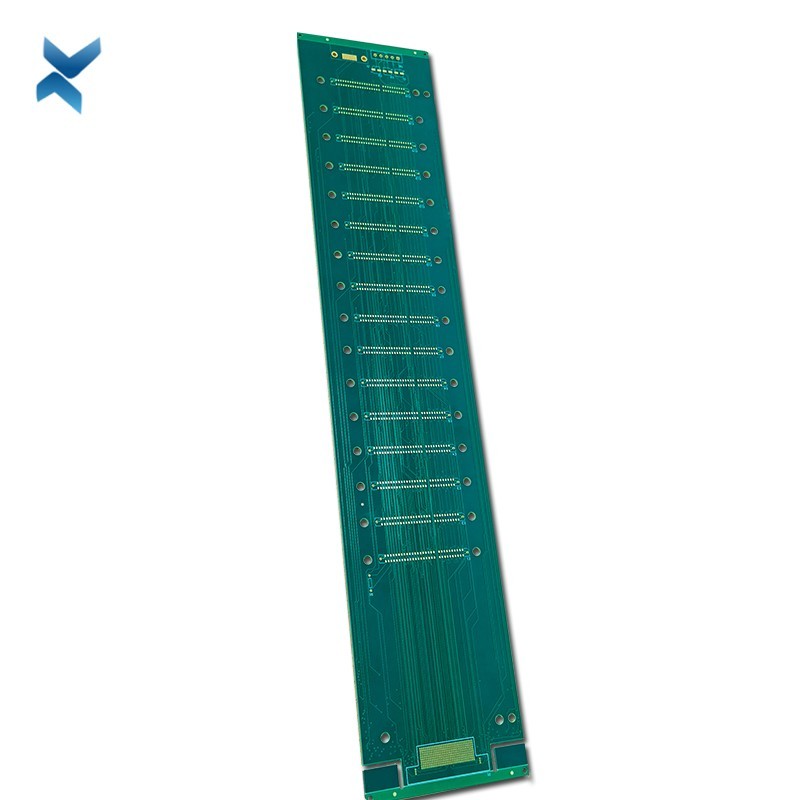
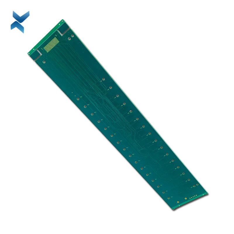
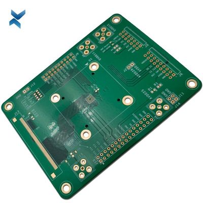
Copper Thickness 3oz HDI PCB Board For Dashboard Electronics

| Place of Origin | Shenzhen |
|---|---|
| Brand Name | YScircuit |
| Certification | ISO9001,UL,REACH, RoHS |
| Model Number | YS-HDI-0014 |
| Minimum Order Quantity | 1 piece |
| Price | 0.04-5$/piece |
| Packaging Details | Foam cotton + carton + strap |
| Delivery Time | 2-8 days |
| Payment Terms | T/T,PayPal, Alibaba pay |
| Supply Ability | 251,000 square meter/year |

Contact me for free samples and coupons.
Whatsapp:0086 18588475571
Wechat: 0086 18588475571
Skype: sales10@aixton.com
If you have any concern, we provide 24-hour online help.
xProduct Details
| Material | FR4 | Size | 60*12cm |
|---|---|---|---|
| Process | Immersion Gold | Surface Finishing | HASL/HASL-LF/ENIG/OSP |
| Copper Thickness | 3oz | Application | Dashboard Electronics |
| Color | 0.25mm(10mil) | TG | 175 |
| High Light | 3oz HDI PCB Board,REACH HDI PCB Board,3oz HDI Printed Circuit Boards |
||
Product Description
Copper Thickness 3oz HDI PCB Board For Dashboard Electronics
HDI Printed Circuit Boards Blind Buried Via Bare Board For Dashboard Electronics
HDI PCB
High density interconnect PCBs are a way of making more room on your PCB to make them more efficient and allow for faster transmission.
It's relatively easy for most enterprising companies that are using printed circuit boards to see how this can benefit them.
High density interconnect (HDI) PCBs represent one of the fastest-growing segments of the PCB market.
Because of its higher circuitry density, the HDI technology can incorporate finer lines and spaces, smaller vias and capture pads, and higher connection pad densities.
A high-density PCB features blind and buried vias and often contains microvias that are .006 in diameter or even less.
Key Benefits of HDI PCB
The evolution of PCB HDI technology has given engineers greater design freedom and flexibility than ever before.
Designers using HDI high density interconnect methods now can place more components on both sides of the raw PCB if desired.
In essence, an HDI PCB gives designers more space to work with, while allowing them to place smaller components even closer together.
This means that a high-density interconnect PCB ultimately results in faster signal transmission along with enhanced signal quality.
HDI PCB is widely used to reduce the weight and overall dimensions of products, as well as to enhance the electrical performance of the device. The high-density PCB is regularly found in mobile phones, touch-screen devices, laptop computers, digital cameras and 4G network communications.
The HDI PCB is also prominently featured in medical devices, as well as various electronic aircraft parts and components.
The possibilities for high-density interconnect PCB technology seem almost limitless.
HDI PCB Applications
HDI boards are appropriate for a wide range of industries.
As mentioned above, you'll find them in all types of digital devices, like smartphones and tablets, where miniaturization is key to the effective application of the product.
You can also find high-density interconnect PCBs in automobiles, aircraft and other vehicles that rely on electronics.
One of the most critical areas where the high-density PCB is making huge inroads is in the medical arena. Medical devices frequently need small packages with high transmission rates that only HDI PCBs can supply. For example, an implant needs to be small enough to fit in the human body, but any electronics involved in that implant absolutely must efficiently allow for high-speed signal transmission. Here, the HDI PCB indeed is a godsend. HDI PCBs can also be useful in other medical equipment, like emergency room monitors, CT scans and much more.
High Density PCBs of Impeccable Quality
Over the course of a decade in business, YScircuit has established a hard-earned reputation for manufacturing PCBs of the highest quality.
Our custom PCB manufacturing capabilities enable you to get the finest quality HDI PCBs at competitive prices without min order quantity requirement.
Our team run design for manufacture check on your custom PCB file and consult with you to ensure it is ready for manufacturing and that your boards will meet your performance requirements.
We also have an on-site quality control department to verify the finished product meet your high quality standards.
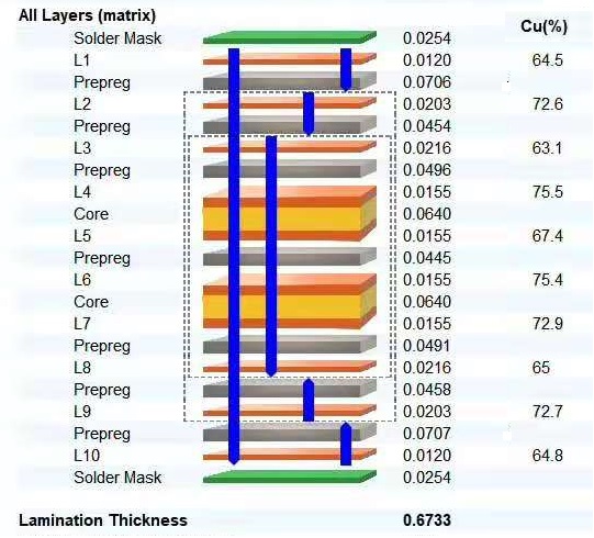
HDI PCB Matrix:
|
YScircuit HDI PCB manufacturing capabilities overview |
|
|
Feature |
capabilities |
|
Layer Count |
4-60L |
|
Available HDI PCB Technology |
1+N+1 |
|
2+N+2 |
|
|
3+N+3 |
|
|
4+N+4 |
|
|
5+N+5 |
|
|
Any layer |
|
|
Thickness |
0.3mm-6mm |
|
Minimum line Width and Space |
0.05mm/0.05mm(2mil/2mil) |
|
BGA PITCH |
0.35mm |
|
Min laser Drilled Size |
0.075mm(3nil) |
|
Min mechanical Drilled Size |
0.15mm(6mil) |
|
Aspect Ratio for laser hole |
0.9:1 |
|
Aspect Ratio for through hole |
16:1 |
|
Surface Finish |
HASL, Lead free HASL,ENIG,Immersion Tin, OSP, Immersion Silver, Gold Finger, Electroplating Hard Gold, Selective OSP,ENEPIG.etc. |
|
Via Fill Option |
The via is plated and filled with either conductive or non-conductive epoxy then capped and plated over |
|
Copper filled, silver filled |
|
|
Laser via copper plated shut |
|
|
Registration |
±4mil |
|
Solder Mask |
Green, Red, Yellow, Blue, White, Black, Purple, Matte Black, Matte green.etc. |
|
layer/m² |
S<1㎡ |
S<3㎡ |
S<6㎡ |
S<10㎡ |
S<13㎡ |
S<16㎡ |
S<20㎡ |
S<30㎡ |
S<40㎡ |
S<50㎡ |
S<65㎡ |
S<85㎡ |
S<100㎡ |
|
1L |
4wds |
6wds |
7wds |
7wds |
9wds |
9wds |
10wds |
10wds |
10wds |
12wds |
14wds |
15wds |
16wds |
|
2L |
4wds |
6wds |
9wds |
9wds |
11wds |
12wds |
13wds |
13wds |
15wds |
15wds |
15wds |
15wds |
18wds |
|
4L |
6wds |
8wds |
12wds |
12wds |
14wds |
14wds |
14wds |
14wds |
15wds |
20wds |
25wds |
25wds |
28wds |
|
6L |
7wds |
9wds |
13wds |
13wds |
17wds |
18wds |
20wds |
22wds |
24wds |
25wds |
26wds |
28wds |
30wds |
|
8L |
9wds |
12wds |
15wds |
18wds |
20wds |
20wds |
22wds |
24wds |
26wds |
27wds |
28wds |
30wds |
30wds |
|
10L |
10wds |
13wds |
17wds |
18wds |
20wds |
20wds |
22wds |
24wds |
26wds |
27wds |
28wds |
30wds |
30wds |
|
12L |
10wds |
15wds |
17wds |
18wds |
20wds |
20wds |
22wds |
24wds |
26wds |
27wds |
28wds |
30wds |
30wds |
|
14L |
10wds |
16wds |
17wds |
18wds |
20wds |
20wds |
22wds |
24wds |
26wds |
27wds |
28wds |
30wds |
30wds |
|
16L |
10wds |
16wds |
17wds |
18wds |
20wds |
20wds |
22wds |
24wds |
26wds |
27wds |
28wds |
30wds |
30wds |
![]()
![]()
![]()
![]()
![]()
FQA
Q: Can you finish PCBs in a shorter time, 2-3 days for example?
A: We can speed up PCB manufacturing and finish the job within 2-3 working days. But there will be rush fees. For expedited PCB production quote, please send your pcb design file and requirements on quantity & lead time to info@yscircuit.com.
Q: How do you calculate lead time for an order?
A: Lead time is counted from the next working day following payment receipt and confirmation of files. It does not include weekends, national holidays and shipping time. Thus, orders placed on Sundays and public holidays will be processed on the next working day.
Q: What is the expected lead time for a PCB?
A: Our lead time for standard circuit boards production is 5-7 working days, and 4-6 working days prototype PCBs. PCB price will be different when selecting different lead time.
Q: What is the lead time for stencils?
A: Our standard lead time for stencils is 1-2 working days after we have confirmed the stencil production file.
Recommended Products