


All Products
Contact Person :
Zhou
Phone Number :
+86 15019457904
Whatsapp :
+8615019457904
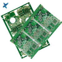
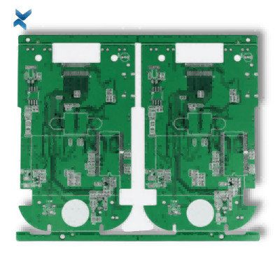
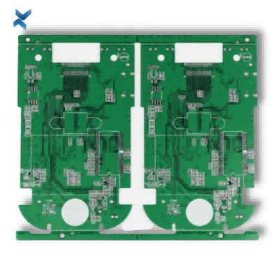
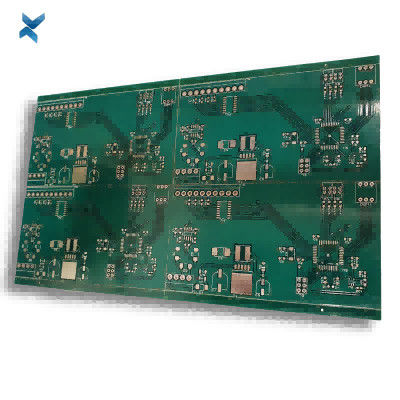
FR4 HDI High Density Interconnect PCB For Engine Control Units


| Place of Origin | Shenzhen |
|---|---|
| Brand Name | YScircuit |
| Certification | ISO9001,UL,REACH, RoHS |
| Model Number | YS-HDI-0013 |
| Minimum Order Quantity | 1 piece |
| Price | 0.04-5$/piece |
| Packaging Details | Foam cotton + carton + strap |
| Delivery Time | 2-8 days |
| Payment Terms | T/T,PayPal, Alibaba pay |
| Supply Ability | 251,000 square meter/year |

Contact me for free samples and coupons.
Whatsapp:0086 18588475571
Wechat: 0086 18588475571
Skype: sales10@aixton.com
If you have any concern, we provide 24-hour online help.
xProduct Details
| Material | FR4 | Size | 23*11cm |
|---|---|---|---|
| Process | Immersion Gold | Surface Finishing | HASL/HASL-LF/ENIG/OSP |
| Copper Thickness | 1oz | Application | Engine Control Units |
| Color | 0.25mm(10mil) | TG | 175 |
| High Light | FR4 High Density Interconnect PCB,1oz High Density PCB,FR4 HDI Circuit Boards |
||
Product Description
FR4 HDI High Density Interconnect PCB For Engine Control Units
High-Tech Blind Buried Via Pcb HDI Printed Circuit Boards For Engine Control Units
What is a HDI PCB?
HDI stands for High Density Interconnector.
A circuit board which has a higher wiring density per unit area as opposed to conventional board is called as HDI PCB. HDI PCBs have finer spaces and lines, minor vias and capture pads and higher connection pad density.
It is helpful in enhancing electrical performance and reduction in weight and size of the equipment.
HDI PCB is the better option for high-layer count and costly laminated boards.
Regarding the electrical needs of high-speed signal, the board should have various features i.e. high-frequency transmission capability, impedance control, decreases redundant radiation, etc.
The board should be enhanced in the density because of the miniaturization and arrays of the electronic parts.
In addition, to the result of the assembling techniques of leadless, fine pitch package and direct chip bonding, the board is even featured with exceptional high-density.
Innumerable benefits are associated with HDI PCB, like high speed, small size and high frequency.
It is the primary part of portable computers, personal computers, and mobile phones.
Currently, HDI PCB is extensively used in other end user products i.e. as MP3 players and game consoles, etc.
HDI PCBs take advantage of the most recent technologies existing to amplify the functionality of circuit boards by means of the similar or little amounts of area.
This development in board technology is motivated by the tininess of parts and semiconductor packages that assist superior characteristics in innovative new products like touch screen tabs.
HDI PCBs are described by high-density features comprising of laser micro-vias, high performance thin materials and fine lines.
The better density allows extra functions per unit area.
These types of multifaceted structures give the required routing resolution for large pin-count chips which are used in mobile devices and other high technology products.
The placement of the parts on the circuit board needs extra precision than conservative board design due to miniature pads and fine pitch of the circuitry on the circuit board.
Leadless chips require special soldering methods and additional steps in the assembly and repair process.
The lesser weight and size of the HDI circuitry means the PCBs fit into the little spaces and have a smaller amount of mass than conservative PCB designs.
The smaller weight and size even signifies that there is lesser chance of harm from mechanical shocks.
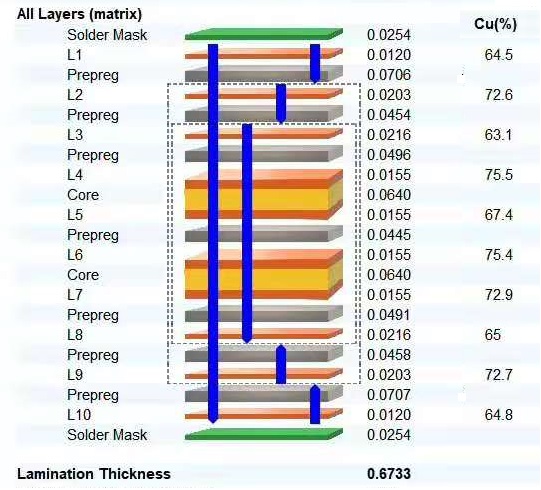
HDI PCB Matrix:
|
YScircuit HDI PCB manufacturing capabilities overview |
|
|
Feature |
capabilities |
|
Layer Count |
4-60L |
|
Available HDI PCB Technology |
1+N+1 |
|
2+N+2 |
|
|
3+N+3 |
|
|
4+N+4 |
|
|
5+N+5 |
|
|
Any layer |
|
|
Thickness |
0.3mm-6mm |
|
Minimum line Width and Space |
0.05mm/0.05mm(2mil/2mil) |
|
BGA PITCH |
0.35mm |
|
Min laser Drilled Size |
0.075mm(3nil) |
|
Min mechanical Drilled Size |
0.15mm(6mil) |
|
Aspect Ratio for laser hole |
0.9:1 |
|
Aspect Ratio for through hole |
16:1 |
|
Surface Finish |
HASL, Lead free HASL,ENIG,Immersion Tin, OSP, Immersion Silver, Gold Finger, Electroplating Hard Gold, Selective OSP,ENEPIG.etc. |
|
Via Fill Option |
The via is plated and filled with either conductive or non-conductive epoxy then capped and plated over |
|
Copper filled, silver filled |
|
|
Laser via copper plated shut |
|
|
Registration |
±4mil |
|
Solder Mask |
Green, Red, Yellow, Blue, White, Black, Purple, Matte Black, Matte green.etc. |
|
layer/m² |
S<1㎡ |
S<3㎡ |
S<6㎡ |
S<10㎡ |
S<13㎡ |
S<16㎡ |
S<20㎡ |
S<30㎡ |
S<40㎡ |
S<50㎡ |
S<65㎡ |
S<85㎡ |
S<100㎡ |
|
1L |
4wds |
6wds |
7wds |
7wds |
9wds |
9wds |
10wds |
10wds |
10wds |
12wds |
14wds |
15wds |
16wds |
|
2L |
4wds |
6wds |
9wds |
9wds |
11wds |
12wds |
13wds |
13wds |
15wds |
15wds |
15wds |
15wds |
18wds |
|
4L |
6wds |
8wds |
12wds |
12wds |
14wds |
14wds |
14wds |
14wds |
15wds |
20wds |
25wds |
25wds |
28wds |
|
6L |
7wds |
9wds |
13wds |
13wds |
17wds |
18wds |
20wds |
22wds |
24wds |
25wds |
26wds |
28wds |
30wds |
|
8L |
9wds |
12wds |
15wds |
18wds |
20wds |
20wds |
22wds |
24wds |
26wds |
27wds |
28wds |
30wds |
30wds |
|
10L |
10wds |
13wds |
17wds |
18wds |
20wds |
20wds |
22wds |
24wds |
26wds |
27wds |
28wds |
30wds |
30wds |
|
12L |
10wds |
15wds |
17wds |
18wds |
20wds |
20wds |
22wds |
24wds |
26wds |
27wds |
28wds |
30wds |
30wds |
|
14L |
10wds |
16wds |
17wds |
18wds |
20wds |
20wds |
22wds |
24wds |
26wds |
27wds |
28wds |
30wds |
30wds |
|
16L |
10wds |
16wds |
17wds |
18wds |
20wds |
20wds |
22wds |
24wds |
26wds |
27wds |
28wds |
30wds |
30wds |
![]()
![]()
![]()
![]()
![]()
FQA
Q: Which software you propose to create a pcb? / What files do you need?
A: You provide us with PCB design files in Gerber, or files in PCB formats.
Q: I need to change the PCB file of my order, how can I do that?
A: You may change the file without cost if the order hasn't been confirmed. Once the order is confirmed and scheduled for production, there will be some scrap fee:
1. If it's a prototype order, the whole order value will be scrapped;
2. If it's a standard PCB order, the scrap fee will be charged based on the production process.
To change your file, please send the updated PCB file along with the order number and PCB part number to info@yscircuit.com. We'll react very quickly.
Q: I need to change BOM of my assembly order. What should I do?
A: Please send the final BOM to info@yscircuit.com. We'll handle the rest.
Q: Can you review my PCB files first? I need to know that you have the capabilities to make my boards before order.
A: We have capabilities to manufacture almost all kinds of circuit boards. Please check our PCB manufacturing capabilities first, then submit the order online. Once payment received, we'll carry out DFM check. We'll be in touch if there's any question on your file.
Q: I only have single PCB file, can you panelize the file and manufacture boards in panels?
A: Yes, we offer PCB file panelization service. Our engineers will panelize the file based on your circuit spec and send you the final panelized file for confirmation.
Recommended Products