


All Products
Contact Person :
Zhou
Phone Number :
+86 15019457904
Whatsapp :
+8615019457904
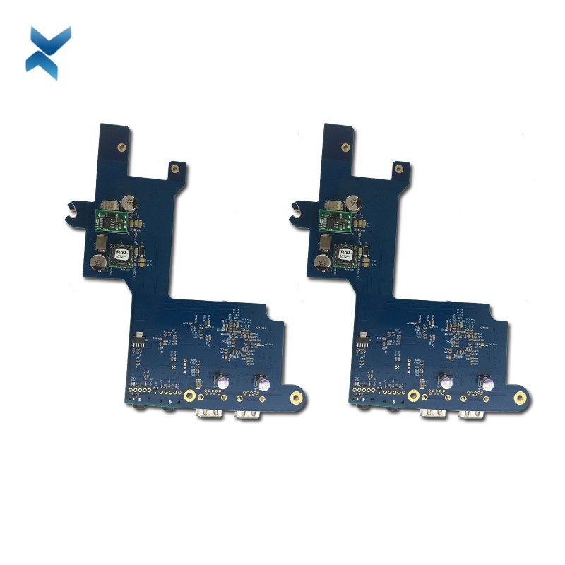
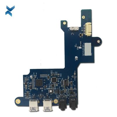
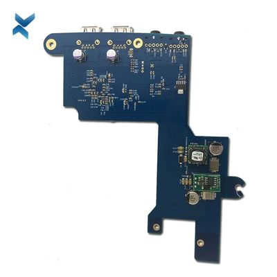
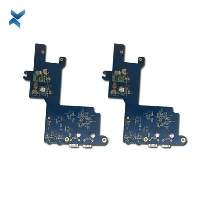
Customized PCBA Circuit Board Assembly FR4 Material With Rohs Certified


| Place of Origin | Shenzhen |
|---|---|
| Brand Name | YScircuit |
| Certification | ISO9001,UL,REACH, RoHS |
| Model Number | YS-PCBA-0004 |
| Minimum Order Quantity | 1 piece |
| Price | 0.04-5$/piece |
| Packaging Details | Foam cotton + carton + strap |
| Delivery Time | 2-8 days |
| Payment Terms | T/T,PayPal, Alibaba pay |
| Supply Ability | 251,000 square meter/year |

Contact me for free samples and coupons.
Whatsapp:0086 18588475571
Wechat: 0086 18588475571
Skype: sales10@aixton.com
If you have any concern, we provide 24-hour online help.
xProduct Details
| Material | FR4 | Size | According To Customer Request |
|---|---|---|---|
| Process | Immersion Gold/sliver/Assembly | Surface Finishing | HASL/HASL-LF/ENIG/OSP |
| Base Material | FR-4 | Copper Thickness | 0.5OZ-6OZ |
| Min. Line Spacing | 0.1mm | Board Thickness | 0.4-2.4 Mm |
| High Light | Customized PCBA Circuit Board Assembly,PCBA Circuit Board Assembly FR4,Rohs Customized Circuit Board |
||
Product Description
Pcba Manufacture Pcb Board Shenzhen Customized Printed Circuit Board With Rohs
PCB Design Basics
The PCBA process always starts out with the most basic unit of the PCB: the base, which consists of several layers, and each one plays a significant role in the functionality of the final PCB. These alternating layers include:
• Substrate: This is the base material of a PCB. It gives the PCB its rigidity.
• Copper: A thin layer of conductive copper foil is added to each functional side of the PCB — on one side if it's a single-sided PCB, and on both sides if it's a double-sided PCB. This is the layer of copper traces.
• Solder mask: On top of the copper layer is the solder mask, which gives each PCB its characteristic green color. It insulates copper traces from unintentionally contacting other conductive materials, which could result in a short. The solder, in other words, keeps everything in its place. Holes in the solder mask are where solder is applied to attach components to the board. Solder mask is a vital step for smooth manufacturing of PCBA since it stops soldering from taking place on unwanted parts with shorts avoided.
• Silkscreen: A white silkscreen is the final layer on a PCB board. This layer adds labels to the PCB in the form of characters and symbols. This helps indicate the function of each component on the board.
SMT PCBA
Surface mount technology allows us to compact designs and utilise PCB space more efficiently. Power handling circuits still need larger components but signal circuitry can seriously shrink in good design.
Our SMT line consists of two pick and place machines, an MPM paste printer and a panasert reflow oven with capacity to load many thousands of parts per 8 hour shift.
Through Hole PCBA
Through hole parts come in radial, axial and multiple lead in many configurations. Before surface mount technology became popular in the 1980s through hole (often spelt thru-hole) was the primary method of PCB assembly for some decades. Usually mass loaded and wave soldered we hand solder through hole components when necessary.
Although generally considered the simplest form of soldering, through hole soldering is best performed by appropriately trained and skilled staff.
Wave Soldering
Our wave soldering machine is fairly standard. PCBs go into special carriers and traverse the conveyor through the flux applicator into pre-heating and finally onto the wave itself. We use non-corrosive flux where possible and the wave soldering machine usually has fairly standard 63/37 solder in it. We offer PCB cleaning, for conformal coating or similar process, but if corrosive flux is used the PCBs must be cleaned anyway.
Considerations to thermal shock, heat sinks (actual and large ground planes with direct connections), thermal sensitivity of some parts and potential contaminants are very important in the wave soldering process
Manual Soldering
Some parts or circumstances call for manual placement and soldering of parts. A part may have thermal profile requirements that preclude it from wave soldering. PCBs with double sided SMT load, where glue was not acceptible, usually have very few through hole parts but they will have to be manually placed and soldered in most cases.
Some (though not many) SMT parts cannot withstand the minimum thermal profile necessary in the reflow oven for the rest of the PCB in question.
| YScircuit HDI PCB manufacturing capabilities overview | |
| Feature | capabilities |
| Layer Count | 4-60L |
| Available HDI PCB Technology | 1+N+1 |
| 2+N+2 | |
| 3+N+3 | |
| 4+N+4 | |
| 5+N+5 | |
| Any layer | |
| Thickness | 0.3mm-6mm |
| Minimum line Width and Space | 0.05mm/0.05mm(2mil/2mil) |
| BGA PITCH | 0.35mm |
| Min laser Drilled Size | 0.075mm(3nil) |
| Min mechanical Drilled Size | 0.15mm(6mil) |
| Aspect Ratio for laser hole | 0.9:1 |
| Aspect Ratio for through hole | 16:1 |
| Surface Finish | HASL, Lead free HASL,ENIG,Immersion Tin, OSP, Immersion Silver, Gold Finger, Electroplating Hard Gold, Selective OSP,ENEPIG.etc. |
| Via Fill Option | The via is plated and filled with either conductive or non-conductive epoxy then capped and plated over |
| Copper filled, silver filled | |
| Laser via copper plated shut | |
| Registration | ±4mil |
| Solder Mask | Green, Red, Yellow, Blue, White, Black, Purple, Matte Black, Matte green.etc. |
![]()
![]()
![]()
![]()
![]()
Recommended Products