


All Products
Contact Person :
Zhou
Phone Number :
+86 15019457904
Whatsapp :
+8615019457904
FR4 Material Electronics PCB PCBA , Assembly Circuit Board With Immersion Gold


| Place of Origin | Shenzhen |
|---|---|
| Brand Name | YScircuit |
| Certification | ISO9001,UL,REACH, RoHS |
| Model Number | YS-PCBA-0003 |
| Minimum Order Quantity | 1 piece |
| Price | 0.04-5$/piece |
| Packaging Details | Foam cotton + carton + strap |
| Delivery Time | 2-8 days |
| Payment Terms | T/T,PayPal, Alibaba pay |
| Supply Ability | 251,000 square meter/year |

Contact me for free samples and coupons.
Whatsapp:0086 18588475571
Wechat: 0086 18588475571
Skype: sales10@aixton.com
If you have any concern, we provide 24-hour online help.
xProduct Details
| Material | FR4 | Process | Immersion Gold/sliver/Assembly |
|---|---|---|---|
| Size | According To Customer Request | Surface Finishing | HASL/HASL-LF/ENIG/OSP |
| High Light | FR4 Electronics PCB PCBA,Electronics PCB PCBA Assembly,Immersion Gold Assembly Circuit Board |
||
Product Description
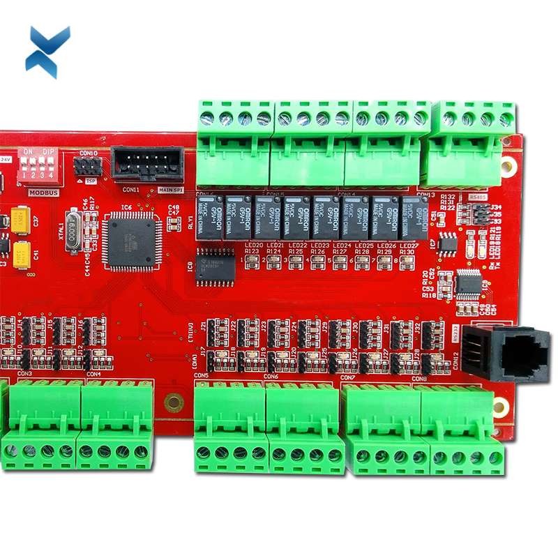
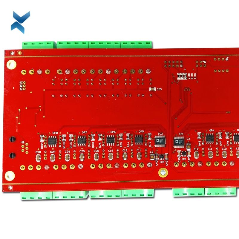
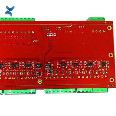
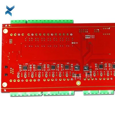
pcba assembly oem shenzhen circuit board printing design and gerber bom file for pcba
Step 1: Solder Paste Stenciling
The first step of PCB assembly is applying a solder paste to the board. This process is like screen-printing a shirt, except instead of a mask, a thin, stainless-steel stencil is placed over the PCB. This allows assemblers to apply solder paste only to certain parts of the would-be PCB. These parts are where components will sit in the finished PCB.
The solder paste itself is a greyish substance consisting of tiny balls of metal, also known as solder. The composition of these tiny metal balls is 96.5% tin, 3% silver and 0.5% copper. The solder paste mixes solder with a flux, which is a chemical designed help the solder melt and bond to a surface. Solder paste appears as a grey paste and must be applied to the board at exactly the right places and in precisely the right amounts.
In a professional PCBA line, a mechanical fixture holds the PCB and solder stencil in place. An applicator then places solder paste on the intended areas in precise amounts. The machine then spreads the paste across the stencil, applying it evenly to every open area. After removing the stencil, the solder paste remains in the intended locations.
Step 2: Pick and Place
After applying the solder paste to the PCB board, the PCBA process moves on to the pick and place machine, a robotic device places surface mount components, or SMDs, on a prepared PCB. SMDs account for most non-connector components on PCBs today. These SMDs are then soldered on to the surface of the board in the next step of PCBA process.
Traditionally, this was a manual process done with a pair of tweezers, in which assemblers had to pick and place components by hand. These days, thankfully, this step is an automated process among PCB manufacturers. This shift occurred largely because machines tend to be more accurate and more consistent than humans. While humans can work quickly, fatigue and eyestrain tends to set in after a few hours working with such small components. Machines work around the clock without such fatigue.
The device starts the pick and place process by picking up a PCB board with a vacuum grip and moving it to the pick and place station. The robot then orients the PCB at the station and begins applying the SMTs to the PCB surface. These components are placed on top of the soldering paste in preprogrammed locations.
Step 3: Reflow Soldering
Once the solder paste and surface mount components are all in place, they need to remain there. This means the solder paste needs to solidify, adhering components to the board. PCB assembly accomplishes this through a process called "reflow".
After the pick and place process concludes, the PCB board is transferred to a conveyor belt. This conveyor belt moves through a large reflow oven, which is somewhat like a commercial pizza oven. This oven consists of a series of heaters which gradually heat the board to temperatures around 250 degrees Celsius, or 480 degrees Fahrenheit. This is hot enough to melt the solder in the solder paste.
| YScircuit HDI PCB manufacturing capabilities overview | |
| Feature | capabilities |
| Layer Count | 4-60L |
| Available HDI PCB Technology | 1+N+1 |
| 2+N+2 | |
| 3+N+3 | |
| 4+N+4 | |
| 5+N+5 | |
| Any layer | |
| Thickness | 0.3mm-6mm |
| Minimum line Width and Space | 0.05mm/0.05mm(2mil/2mil) |
| BGA PITCH | 0.35mm |
| Min laser Drilled Size | 0.075mm(3nil) |
| Min mechanical Drilled Size | 0.15mm(6mil) |
| Aspect Ratio for laser hole | 0.9:1 |
| Aspect Ratio for through hole | 16:1 |
| Surface Finish | HASL, Lead free HASL,ENIG,Immersion Tin, OSP, Immersion Silver, Gold Finger, Electroplating Hard Gold, Selective OSP,ENEPIG.etc. |
| Via Fill Option | The via is plated and filled with either conductive or non-conductive epoxy then capped and plated over |
| Copper filled, silver filled | |
| Laser via copper plated shut | |
| Registration | ±4mil |
| Solder Mask | Green, Red, Yellow, Blue, White, Black, Purple, Matte Black, Matte green.etc. |
| layer/m² | S<1㎡ | S<3㎡ | S<6㎡ | S<10㎡ | S<13㎡ | S<16㎡ | S<20㎡ | S<30㎡ | S<40㎡ | S<50㎡ | S<65㎡ | S<85㎡ | S<100㎡ |
| 1L | 4wds | 6wds | 7wds | 7wds | 9wds | 9wds | 10wds | 10wds | 10wds | 12wds | 14wds | 15wds | 16wds |
| 2L | 4wds | 6wds | 9wds | 9wds | 11wds | 12wds | 13wds | 13wds | 15wds | 15wds | 15wds | 15wds | 18wds |
| 4L | 6wds | 8wds | 12wds | 12wds | 14wds | 14wds | 14wds | 14wds | 15wds | 20wds | 25wds | 25wds | 28wds |
| 6L | 7wds | 9wds | 13wds | 13wds | 17wds | 18wds | 20wds | 22wds | 24wds | 25wds | 26wds | 28wds | 30wds |
| 8L | 9wds | 12wds | 15wds | 18wds | 20wds | 20wds | 22wds | 24wds | 26wds | 27wds | 28wds | 30wds | 30wds |
| 10L | 10wds | 13wds | 17wds | 18wds | 20wds | 20wds | 22wds | 24wds | 26wds | 27wds | 28wds | 30wds | 30wds |
| 12L | 10wds | 15wds | 17wds | 18wds | 20wds | 20wds | 22wds | 24wds | 26wds | 27wds | 28wds | 30wds | 30wds |
| 14L | 10wds | 16wds | 17wds | 18wds | 20wds | 20wds | 22wds | 24wds | 26wds | 27wds | 28wds | 30wds | 30wds |
| 16L | 10wds | 16wds | 17wds | 18wds | 20wds | 20wds | 22wds | 24wds | 26wds | 27wds | 28wds | 30wds | 30wds |
![]()
![]()
![]()
![]()
![]()
Recommended Products