


All Products
Contact Person :
Zhou
Phone Number :
+86 15019457904
Whatsapp :
+8615019457904
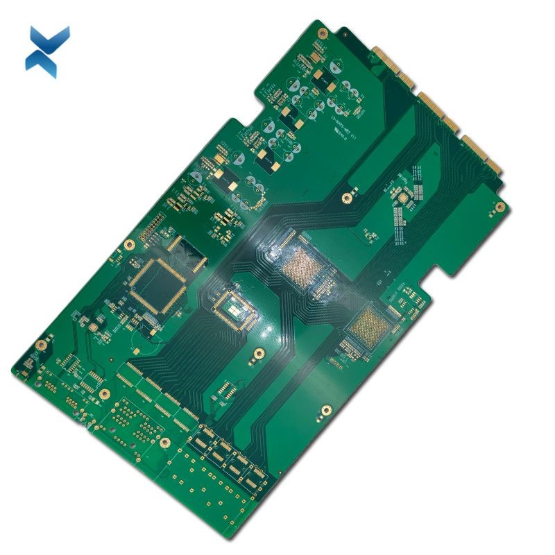
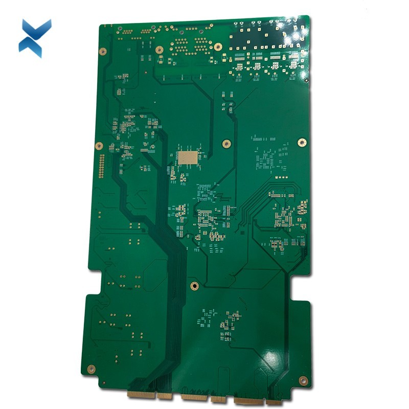
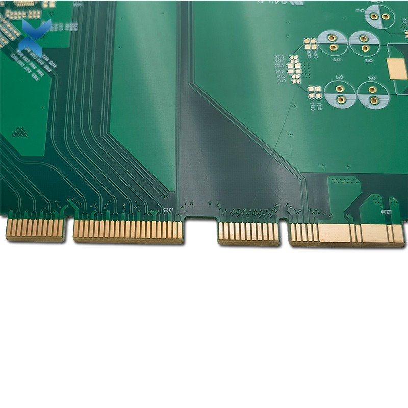
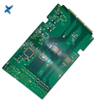
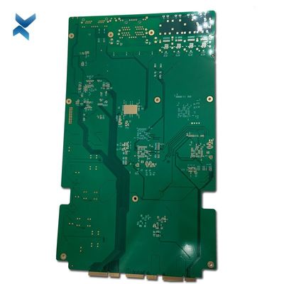
Polyimide PCB Multilayer Printed Circuit Boards For Anti Aging Test
| Place of Origin | Shenzhen |
|---|---|
| Brand Name | YScircuit |
| Certification | ISO9001,UL,REACH, RoHS |
| Model Number | YS-ML-0022 |
| Minimum Order Quantity | 1 |
| Price | $0.09-6.8/piece |
| Packaging Details | Foam cotton + carton + strap |
| Delivery Time | 2-8 work days |
| Payment Terms | T/T,PayPal, Alibaba pay |
| Supply Ability | 1580000 |

Contact me for free samples and coupons.
Whatsapp:0086 18588475571
Wechat: 0086 18588475571
Skype: sales10@aixton.com
If you have any concern, we provide 24-hour online help.
xProduct Details
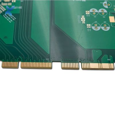
| Product Name | 2 Layer PCB | Surface Finishing | HASL/HASL-LF/ENIG/OSP |
|---|---|---|---|
| Process | Immersion Gold | Copper Thickness | 2 Oz |
| Board Thickness | 1.2mm | Application | An-ti Aging Test |
| Raw Color | Light Yellow | Size | 320*180mm |
| High Light | Anti Aging Test Polyimide PCB,1.2mm Multilayer Printed Circuit Boards,Multilayer Polyimide PCB |
||
Product Description
Polyimide PCB Multilayer Printed Circuit Boards For An-Ti Aging Test
Multilayer PCB Applications
The advantages and comparisons discussed above beg the question: what's the use of multilayer PCBs in real world?
The answer is just about any use.
For numerous industries, multilayer PCBs have become the preferred option for a variety of applications.
Much of this preference derives from the continuous push across all technology toward mobility and functionality.
Multilayer PCBs are the logical step in this progression, achieving greater functionality while reducing size.
As such, they've become fairly ubiquitous, used in many technologies including:
• Consumer Electronics: Consumer electronics is a broad term used to cover a wide range of products used by the general public.
This tends to include products used on a daily basis, such as smartphones and microwaves.
Each of these consumer electronics contains a PCB, but an increasing proportion of them are using multilayer PCBs instead of standard single layers.
Why? Most of the reason lies in consumer trends.
People in the modern world tend to prefer multi-function gadgets and smart devices that integrate with the rest of their lives.
From universal remotes to smartwatches, these types of devices are fairly common in the modern world.
They also tend to use multilayer PCBs for their increased functionality and smaller size.
Consumer Electronics Multilayer PCBs
• Computer Electronics: Everything from servers to motherboards uses multilayer PCBs, primarily for their space-saving attributes and high functionality.
With these applications, performance is one of the most essential characteristics of a PCB, whereas cost is relatively low on the list of priorities.
As such, multilayer PCBs are an ideal solution for many technologies in this industry.
• Telecommunications: Telecommunication devices often use multilayer PCBs in numerous general applications, such as signal transmission, GPS and satellite applications.
The reason for this lies primarily in their durability and functionality.
PCBs for telecommunications applications are often either used in mobile devices or towers outdoors.
In such applications, durability is essential while still maintaining a high level of functionality.
• Industrial: Multilayer PCBs do prove more durable than several other options currently on the market, making them a good choice for applications where rough handling may be a daily occurrence.
As such, multilayer PCBs have become popular in several industrial applications, most notable of which are industrial controls.
From industrial computers to control systems, multilayer PCBs are used throughout manufacturing and industrial applications to run machinery, favored for their durability as well as their small size and functionality.
• Medical Devices: Electronics is becoming an increasingly essential part of the healthcare industry, functioning in every corner of the industry from treatment to diagnosis.
Multilayer PCBs are particularly favored in Medical industry for their small size, lightweight nature and impressive functionality compared to single-layer alternatives.
These benefits have led to multilayer PCBs being used in modern X-ray equipment, heart monitors, CAT scan equipment and medical testing devices etc.
Medical Device Multilayer PCBs
• Military and Defense: Favored for their durability, functionality and low weight, multilayer PCBs are useful in high-speed circuits, which is becoming an increasing priority for military applications.
They're also favored due to the defense industry's increased movement toward highly compact engineering designs, as the small size of multilayer PCBs leaves more room for other components to flourish existing functions.
• Automotive: Cars are relying on electronic components more and more in the modern era, especially with the rise of electric cars.
With everything from GPS's and onboard computers to headlight switches and engine sensors controlled by electronics, using the right kinds of components becomes increasingly essential in automotive design.
This's why many auto manufacturers start to favor multilayer PCBs over other alternatives.
While they are small and durable, multilayer PCBs are also highly functional and relatively heat-resistant, making them a good fit for the internal environment of an automobile.
• Aerospace: Like cars, jets and rockets rely heavily on electronics in the modern era, all of which must be extremely precise.
From the computers used on the ground to those used in the cockpit, aerospace PCB applications must be reliable, able to handle the stresses of atmospheric journeys while simultaneously making enough room for the rest of the surrounding equipment.
Multilayer PCBs present an ideal solution in this case, with plenty of protective layers to keep heat and outside stress from damaging the connections, as well as the ability to be made from flexible materials.
Their higher quality and functionality also contributes to this utility in the aerospace industry, as aerospace companies prefer to use the best materials possible to keep their personnel and equipment safe.
• And Many More! Multilayer PCBs are used in a wide variety of other industries, including the science and research industry and even home appliances and security.
Everything from alarm systems and fiber optic sensors to atomic accelerators and weather analysis equipment uses multilayer PCBs, taking advantage of the space and weight savings offered by this PCB format, as well as their heightened functionality.
| YS Multilayer PCB manufacturing capabilities overview | ||
| Feature | capabilities | |
| Layer Count | 2-60L | |
| Available Multilayer PCB Technology | Through hole with Aspect Ratio 16:1 | |
| buried and blind via | ||
| Hybrid | High Frequency Material such as RO4350B and FR4 Mix etc. | |
| High Speed Material such as M7NE and FR4 Mix etc. | ||
| Thickness | 0.3mm-8mm | |
| Minimum line Width and Space | 0.05mm/0.05mm(2mil/2mil) | |
| BGA PITCH | 0.35mm | |
| Min mechanical Drilled Size | 0.15mm(6mil) | |
| Aspect Ratio for through hole | 10:1 | |
| Surface Finish | HASL, Lead free HASL,ENIG,Immersion Tin, OSP, Immersion Silver, Gold Finger, Electroplating Hard Gold, Selective OSP,ENEPIG.etc. | |
| Via Fill Option | The via is plated and filled with either conductive or non-conductive epoxy then capped and plated over(VIPPO) | |
| Copper filled, silver filled | ||
| Registration | ±4mil | |
| Solder Mask | Green, Red, Yellow,White, Black, Purple, Matte Black, Matte green.etc. | |
| layer/m² | S<1㎡ | S<3㎡ | S<6㎡ | S<10㎡ | S<13㎡ | S<16㎡ | S<20㎡ | S<30㎡ | S<40㎡ | S<50㎡ | S<65㎡ | S<85㎡ | S<100㎡ |
| 1L | 4wds | 6wds | 7wds | 7wds | 9wds | 9wds | 10wds | 10wds | 10wds | 12wds | 14wds | 15wds | 16wds |
| 2L | 4wds | 6wds | 9wds | 9wds | 11wds | 12wds | 13wds | 13wds | 15wds | 15wds | 15wds | 15wds | 18wds |
| 4L | 6wds | 8wds | 12wds | 12wds | 14wds | 14wds | 14wds | 14wds | 15wds | 20wds | 25wds | 25wds | 28wds |
| 6L | 7wds | 9wds | 13wds | 13wds | 17wds | 18wds | 20wds | 22wds | 24wds | 25wds | 26wds | 28wds | 30wds |
| 8L | 9wds | 12wds | 15wds | 18wds | 20wds | 20wds | 22wds | 24wds | 26wds | 27wds | 28wds | 30wds | 30wds |
| 10L | 10wds | 13wds | 17wds | 18wds | 20wds | 20wds | 22wds | 24wds | 26wds | 27wds | 28wds | 30wds | 30wds |
| 12L | 10wds | 15wds | 17wds | 18wds | 20wds | 20wds | 22wds | 24wds | 26wds | 27wds | 28wds | 30wds | 30wds |
| 14L | 10wds | 16wds | 17wds | 18wds | 20wds | 20wds | 22wds | 24wds | 26wds | 27wds | 28wds | 30wds | 30wds |
| 16L | 10wds | 16wds | 17wds | 18wds | 20wds | 20wds | 22wds | 24wds | 26wds | 27wds | 28wds | 30wds | 30wds |
![]()
![]()
![]()
![]()
![]()
FQA
Q: What is impedance control in PCB design?
A: Impedance control is the process of maintaining a consistent electrical impedance throughout the length of a trace on a PCB. It is important for high-speed signals to prevent signal distortion and ensure signal integrity.
Q: What is the lead time for manufacturing a PCB?
A: The lead time for manufacturing a PCB can vary depending on the complexity of the design and the chosen manufacturing process, but typically ranges from a few days to a few weeks.
Q: What is the difference between through-hole and surface-mount technology (SMT)?
A: Through-hole technology involves inserting electronic components through holes in the PCB and soldering them in place. SMT involves attaching components directly onto the surface of the PCB using solder paste and a reflow oven.
Q: What is the purpose of a solder mask on a PCB?
A: The solder mask is a protective layer that is applied to the PCB to prevent solder from accidentally bridging between adjacent pads, shorting out the circuit, and causing electrical problems. It also helps to protect the PCB from environmental factors such as moisture and dust .
Q: What is the purpose of a silk screen on a PCB?
A: The silk screen is a layer of printing that is applied to the surface of the PCB to label components and provide other information such as the company logo, part numbers, and test points.
Recommended Products