


All Products
Contact Person :
Zhou
Phone Number :
+86 15019457904
Whatsapp :
+8615019457904
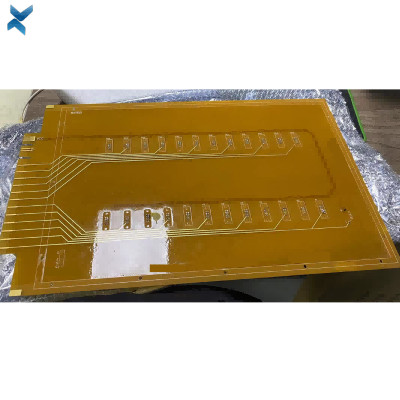
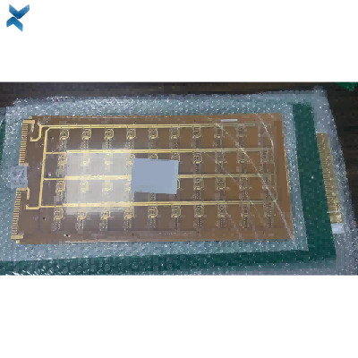
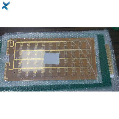
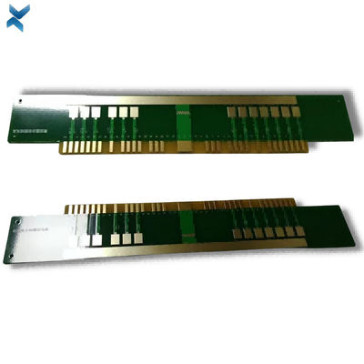
Immersion Gold Multilayer PCB Circuit Board 4 Layer Polyimide


| Place of Origin | Shenzhen |
|---|---|
| Brand Name | YScircuit |
| Certification | ISO9001,UL,REACH, RoHS |
| Model Number | YS-ML-0025 |
| Minimum Order Quantity | 1 |
| Price | $0.09-6.8/piece |
| Packaging Details | Foam cotton + carton + strap |
| Delivery Time | 2-8 work days |
| Payment Terms | T/T,PayPal, Alibaba pay |
| Supply Ability | 1580000 |

Contact me for free samples and coupons.
Whatsapp:0086 18588475571
Wechat: 0086 18588475571
Skype: sales10@aixton.com
If you have any concern, we provide 24-hour online help.
xProduct Details
| Product Name | 4 Layer PCB | Surface Finishing | ENIG 1oz |
|---|---|---|---|
| Process | Immersion Gold | Copper Thickness | 2 Oz |
| Board Thickness | 2mm | Application | Aging Test Board |
| Raw Color | Brown | Size | 40*18cm |
| High Light | Immersion Gold Multilayer PCB Circuit Board,Polyimide Multilayer PCB Circuit Board,Multilayer Amplifier Board PCB |
||
Product Description
Immersion Gold Multilayer PCB Circuit Board 4 Layer Polyimide
VT901 Amplifier Board Pcb YScircuit Pcb 4 Layer Polyimide Aging Test Board
VT901 GENERAL INFORMATION
Tg at 250°C
High thermal stability
Enhanced resistance to cracking
Low coefficient of thermal expansion in the Z-axis
Complies with NASA's regulations regarding bromine visibility
Application:
Suitable for chip manufacturing
Ideal for engine and flight control systems
Perfect for power supply and backplane applications
Well-suited for military and burn-in boards
Availability:
Available in sheet or panel form with core thickness ranging from 0.002" (0.05mm) to 0.125" (3mm)
Copper foil options include 1/4oz to 6oz
Prepregs can be obtained in roll or panel form
Various E-Glass styles available, such as 7628, 1506, 2113, 2313, 3313, 2116, 1080, 106, and more.
|
YS Multilayer PCB manufacturing capabilities overview |
||
|
Feature |
capabilities |
|
|
Layer Count |
2-60L |
|
|
Available Multilayer PCB Technology |
Through hole with Aspect Ratio 16:1 |
|
|
buried and blind via |
||
|
Hybrid |
High Frequency Material such as RO4350B and FR4 Mix etc. |
|
|
High Speed Material such as M7NE and FR4 Mix etc. |
||
|
Thickness |
0.3mm-8mm |
|
|
Minimum line Width and Space |
0.05mm/0.05mm(2mil/2mil) |
|
|
BGA PITCH |
0.35mm |
|
|
Min mechanical Drilled Size |
0.15mm(6mil) |
|
|
Aspect Ratio for through hole |
10:1 |
|
|
Surface Finish |
HASL, Lead free HASL,ENIG,Immersion Tin, OSP, Immersion Silver, Gold Finger, Electroplating Hard Gold, Selective OSP,ENEPIG.etc. |
|
|
Via Fill Option |
The via is plated and filled with either conductive or non-conductive epoxy then capped and plated over(VIPPO) |
|
|
Copper filled, silver filled |
||
|
Registration |
±4mil |
|
|
Solder Mask |
Green, Red, Yellow,White, Black, Purple, Matte Black, Matte green.etc. |
|
|
layer/m² |
S<1㎡ |
S<3㎡ |
S<6㎡ |
S<10㎡ |
S<13㎡ |
S<16㎡ |
S<20㎡ |
S<30㎡ |
S<40㎡ |
S<50㎡ |
S<65㎡ |
S<85㎡ |
S<100㎡ |
|
1L |
4wds |
6wds |
7wds |
7wds |
9wds |
9wds |
10wds |
10wds |
10wds |
12wds |
14wds |
15wds |
16wds |
|
2L |
4wds |
6wds |
9wds |
9wds |
11wds |
12wds |
13wds |
13wds |
15wds |
15wds |
15wds |
15wds |
18wds |
|
4L |
6wds |
8wds |
12wds |
12wds |
14wds |
14wds |
14wds |
14wds |
15wds |
20wds |
25wds |
25wds |
28wds |
|
6L |
7wds |
9wds |
13wds |
13wds |
17wds |
18wds |
20wds |
22wds |
24wds |
25wds |
26wds |
28wds |
30wds |
|
8L |
9wds |
12wds |
15wds |
18wds |
20wds |
20wds |
22wds |
24wds |
26wds |
27wds |
28wds |
30wds |
30wds |
|
10L |
10wds |
13wds |
17wds |
18wds |
20wds |
20wds |
22wds |
24wds |
26wds |
27wds |
28wds |
30wds |
30wds |
|
12L |
10wds |
15wds |
17wds |
18wds |
20wds |
20wds |
22wds |
24wds |
26wds |
27wds |
28wds |
30wds |
30wds |
|
14L |
10wds |
16wds |
17wds |
18wds |
20wds |
20wds |
22wds |
24wds |
26wds |
27wds |
28wds |
30wds |
30wds |
|
16L |
10wds |
16wds |
17wds |
18wds |
20wds |
20wds |
22wds |
24wds |
26wds |
27wds |
28wds |
30wds |
30wds |
![]()
![]()
![]()
![]()
![]()
FQA
What is a Multilayer PCB?
A Multilayer PCB is a printed circuit board that has more than two layers of conductive material separated by insulating layers.
What are the benefits of using a Multilayer PCB?
Multilayer PCBs offer several benefits, such as reduced size and weight, increased functionality, improved performance, and enhanced reliability.
How are Multilayer PCBs manufactured?
Multilayer PCBs are manufactured by layering sheets of conductive material and insulating material together, then laminating and pressing them under heat and pressure.
This process is repeated until the desired number of layers is achieved.
What is the typical number of layers in a Multilayer PCB?
The number of layers in a Multilayer PCB varies depending on the complexity of the circuit design.
Multilayer PCBs can have anywhere from 4 to more than 100 layers.
What is the difference between a Multilayer PCB and a double-sided PCB?
A Multilayer PCB has more than two layers of conductive material separated by insulating layers, while a double-sided PCB has only two layers of conductive material.
What is the maximum number of layers that can be used in a Multilayer PCB?
The maximum number of layers that can be used in a Multilayer PCB is determined by the manufacturing process and the materials used. Typically, Multilayer PCBs have between 4 and 32 layers.
Recommended Products