


All Products
Contact Person :
Zhou
Phone Number :
+86 15019457904
Whatsapp :
+8615019457904
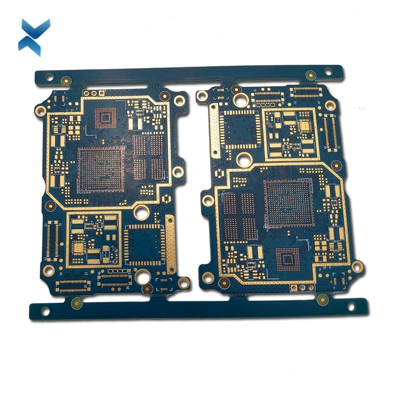
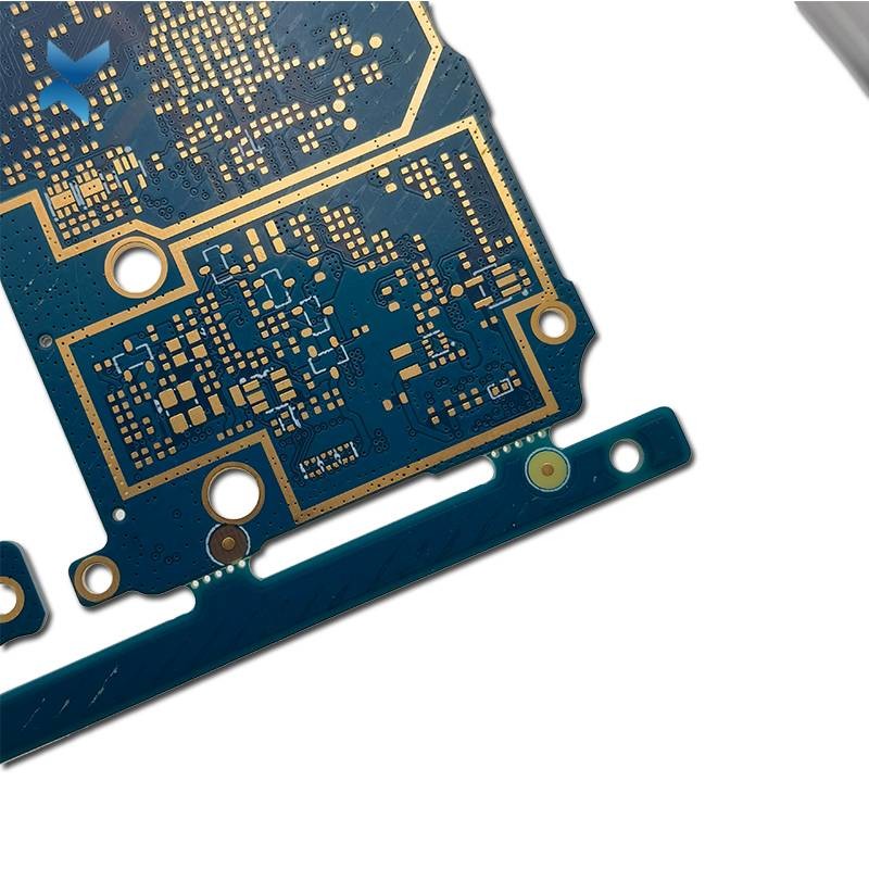
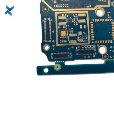
Audio Amplifier Multilayer PCB Circuit Board Fabrication Volume Production


| Place of Origin | Shenzhen |
|---|---|
| Brand Name | YScircuit |
| Certification | ISO9001,UL,REACH, RoHS |
| Model Number | YS-ML-0027 |
| Minimum Order Quantity | 1 |
| Price | $0.09-6.8/piece |
| Packaging Details | Foam cotton + carton + strap |
| Delivery Time | 2-8 work days |
| Payment Terms | T/T,PayPal, Alibaba pay |
| Supply Ability | 1580000 |

Contact me for free samples and coupons.
Whatsapp:0086 18588475571
Wechat: 0086 18588475571
Skype: sales10@aixton.com
If you have any concern, we provide 24-hour online help.
xProduct Details
| Product Name | 2 Layer PCB | Surface Finishing | Immersion Gold |
|---|---|---|---|
| Process | Mass Production | Copper Thickness | Half Oz |
| Board Thickness | 0.8 Mm | Application | Audio Amplifier |
| Raw Color | Black | Size | 26*22cm |
| High Light | Audio Amplifier Multilayer PCB Circuit Board,Half Oz Multilayer PCB Circuit Board,Audio Amplifier Bare Board Fabrication |
||
Product Description
Audio Amplifier Multilayer PCB Circuit Board Fabrication Volume Production
Bare Board Fabrication PCB Volume Production For Audio Amplifier
Advantages of Multilayer PCBs
What do these factors mean when deciding between a multilayer and single layer construction?
Essentially, if you're looking to produce a small, lightweight and complex device where quality is essential, a multilayer PCB is likely your best choice.
However, if size and weight are not primary factors in your product design, then a single or double layer PCB design may be more cost-effective.
|
YS Multilayer PCB manufacturing capabilities overview |
||
|
Feature |
capabilities |
|
|
Layer Count |
2-60L |
|
|
Available Multilayer PCB Technology |
Through hole with Aspect Ratio 16:1 |
|
|
buried and blind via |
||
|
Hybrid |
High Frequency Material such as RO4350B and FR4 Mix etc. |
|
|
High Speed Material such as M7NE and FR4 Mix etc. |
||
|
Thickness |
0.3mm-8mm |
|
|
Minimum line Width and Space |
0.05mm/0.05mm(2mil/2mil) |
|
|
BGA PITCH |
0.35mm |
|
|
Min mechanical Drilled Size |
0.15mm(6mil) |
|
|
Aspect Ratio for through hole |
10:1 |
|
|
Surface Finish |
HASL, Lead free HASL,ENIG,Immersion Tin, OSP, Immersion Silver, Gold Finger, Electroplating Hard Gold, Selective OSP,ENEPIG.etc. |
|
|
Via Fill Option |
The via is plated and filled with either conductive or non-conductive epoxy then capped and plated over(VIPPO) |
|
|
Copper filled, silver filled |
||
|
Registration |
±4mil |
|
|
Solder Mask |
Green, Red, Yellow,White, Black, Purple, Matte Black, Matte green.etc. |
|
|
layer/m² |
S<1㎡ |
S<3㎡ |
S<6㎡ |
S<10㎡ |
S<13㎡ |
S<16㎡ |
S<20㎡ |
S<30㎡ |
S<40㎡ |
S<50㎡ |
S<65㎡ |
S<85㎡ |
S<100㎡ |
|
1L |
4wds |
6wds |
7wds |
7wds |
9wds |
9wds |
10wds |
10wds |
10wds |
12wds |
14wds |
15wds |
16wds |
|
2L |
4wds |
6wds |
9wds |
9wds |
11wds |
12wds |
13wds |
13wds |
15wds |
15wds |
15wds |
15wds |
18wds |
|
4L |
6wds |
8wds |
12wds |
12wds |
14wds |
14wds |
14wds |
14wds |
15wds |
20wds |
25wds |
25wds |
28wds |
|
6L |
7wds |
9wds |
13wds |
13wds |
17wds |
18wds |
20wds |
22wds |
24wds |
25wds |
26wds |
28wds |
30wds |
|
8L |
9wds |
12wds |
15wds |
18wds |
20wds |
20wds |
22wds |
24wds |
26wds |
27wds |
28wds |
30wds |
30wds |
|
10L |
10wds |
13wds |
17wds |
18wds |
20wds |
20wds |
22wds |
24wds |
26wds |
27wds |
28wds |
30wds |
30wds |
|
12L |
10wds |
15wds |
17wds |
18wds |
20wds |
20wds |
22wds |
24wds |
26wds |
27wds |
28wds |
30wds |
30wds |
|
14L |
10wds |
16wds |
17wds |
18wds |
20wds |
20wds |
22wds |
24wds |
26wds |
27wds |
28wds |
30wds |
30wds |
|
16L |
10wds |
16wds |
17wds |
18wds |
20wds |
20wds |
22wds |
24wds |
26wds |
27wds |
28wds |
30wds |
30wds |
![]()
![]()
![]()
![]()
![]()
FQA
Q: What is impedance control in PCB design?
A: Impedance control is the process of maintaining a consistent electrical impedance throughout the length of a trace on a PCB. It is important for high-speed signals to prevent signal distortion and ensure signal integrity.
Q: What is the lead time for manufacturing a PCB?
A: The lead time for manufacturing a PCB can vary depending on the complexity of the design and the chosen manufacturing process, but typically ranges from a few days to a few weeks.
Q: What is the difference between through-hole and surface-mount technology (SMT)?
A: Through-hole technology involves inserting electronic components through holes in the PCB and soldering them in place. SMT involves attaching components directly onto the surface of the PCB using solder paste and a reflow oven.
Q: What is the purpose of a solder mask on a PCB?
A: The solder mask is a protective layer that is applied to the PCB to prevent solder from accidentally bridging between adjacent pads, shorting out the circuit, and causing electrical problems. It also helps to protect the PCB from environmental factors such as moisture and dust .
Q: What is the purpose of a silk screen on a PCB?
A: The silk screen is a layer of printing that is applied to the surface of the PCB to label components and provide other information such as the company logo, part numbers, and test points.
Recommended Products