


All Products
Contact Person :
Zhou
Phone Number :
+86 15019457904
Whatsapp :
+8615019457904
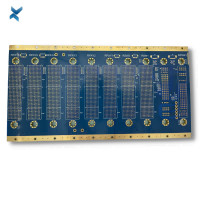
High End Printed Circuit Board 2 Layers PCB For Medical Devices


| Place of Origin | Shenzhen |
|---|---|
| Brand Name | YScircuit |
| Certification | ISO9001,UL,REACH, RoHS |
| Model Number | YS-ML-0021 |
| Minimum Order Quantity | 1 |
| Price | $0.04-7/piece |
| Packaging Details | Foam cotton + carton + strap |
| Delivery Time | 2-8 work days |
| Payment Terms | T/T,PayPal, Alibaba pay |
| Supply Ability | 1580000 |

Contact me for free samples and coupons.
Whatsapp:0086 18588475571
Wechat: 0086 18588475571
Skype: sales10@aixton.com
If you have any concern, we provide 24-hour online help.
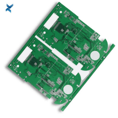
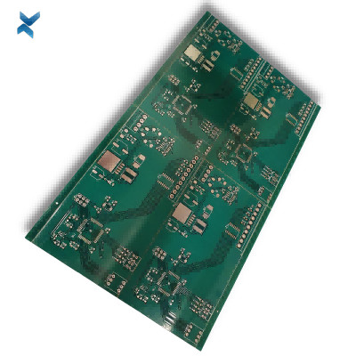
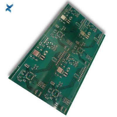
xProduct Details
| Product Name | 2 Layer PCB | Surface Finishing | HASL/HASL-LF/ENIG/OSP |
|---|---|---|---|
| Process | Immersion Gold | Copper Thickness | 2 Oz |
| Board Thickness | 1.2mm | Application | Medical Devices |
| Color | Dark Blue | Size | 200*80mm |
| High Light | 200*80mm Printed Circuit Board,Immersion Gold 2 Layers PCB,Medical Devices 2 Layers PCB |
||
Product Description
High-End Printed Circuit Board 2 Layers PCB For Medical Devices
Why Are Multilayer PCBs So Widely Used?
The specific applications listed above represent only a fraction of multilayer PCBs applied throughout the industry.
But why are they used so widely?
Multilayer PCB Industry Applications
Much of the favoritism toward multilayer PCBs lies in industry trends.
With electronics progressing ever toward miniaturization yet multi-functional options, the internal components of those electronics must follow the same trend.
While single and double-sided PCBs have proven limited in their ability to balance size and functionality, multilayer PCBs provide a comprehensive solution.
While there are several drawbacks to using multilayer PCBs over single and double-layer options, such as increased costs, design times and production inputs, these costs are becoming more accepted in today's world.
Functionality is largely favored over cost, and people are willing to pay more for high capacity electronics.
Additionally, as the technology becomes increasingly mainstream, production techniques and machinery will eventually become less expensive, especially as new techniques arrive in the industry.
PCB Cost vs Functionality
With those irreversible trends and continuing progress of technology, many expect to see multilayer PCBs become even more abundant in the future.
Multilayer PCB Manufacturing and Assembly at Favorable Prices with YScircuit
With technology continuing to progress and the number of multilayer PCB uses expected to expand, your company needs to invest in those trends and increase your focus on multilayer solutions.
Part of this increased focus should include partnering with a quality multilayer PCB manufacturer and assembler.
With such a solution, your company will be perfectly poised to handle any multilayer PCB project that comes your way.YScircuit can help you get there.
YScircuit is a custom PCB solutions provider, serving companies across the world in PCB manufacturing and assembly services.
We help companies from parts sourcing to testing, all the while remaining compliant with IPC Class 3, RoHS and ISO9001:2008 standards.
We'll be with you every step of the way throughout the process of producing your multilayer PCB, providing expertise and advice when needed.
Our experienced team has produced thousands of multilayer PCBs varying in design and complexity.
No matter how intricate the design or how extensive your needs, YScircuit can help.
| YS Multilayer PCB manufacturing capabilities overview | ||
| Feature | capabilities | |
| Layer Count | 2-60L | |
| Available Multilayer PCB Technology | Through hole with Aspect Ratio 16:1 | |
| buried and blind via | ||
| Hybrid | High Frequency Material such as RO4350B and FR4 Mix etc. | |
| High Speed Material such as M7NE and FR4 Mix etc. | ||
| Thickness | 0.3mm-8mm | |
| Minimum line Width and Space | 0.05mm/0.05mm(2mil/2mil) | |
| BGA PITCH | 0.35mm | |
| Min mechanical Drilled Size | 0.15mm(6mil) | |
| Aspect Ratio for through hole | 10:1 | |
| Surface Finish | HASL, Lead free HASL,ENIG,Immersion Tin, OSP, Immersion Silver, Gold Finger, Electroplating Hard Gold, Selective OSP,ENEPIG.etc. | |
| Via Fill Option | The via is plated and filled with either conductive or non-conductive epoxy then capped and plated over(VIPPO) | |
| Copper filled, silver filled | ||
| Registration | ±4mil | |
| Solder Mask | Green, Red, Yellow,White, Black, Purple, Matte Black, Matte green.etc. | |
| layer/m² | S<1㎡ | S<3㎡ | S<6㎡ | S<10㎡ | S<13㎡ | S<16㎡ | S<20㎡ | S<30㎡ | S<40㎡ | S<50㎡ | S<65㎡ | S<85㎡ | S<100㎡ |
| 1L | 4wds | 6wds | 7wds | 7wds | 9wds | 9wds | 10wds | 10wds | 10wds | 12wds | 14wds | 15wds | 16wds |
| 2L | 4wds | 6wds | 9wds | 9wds | 11wds | 12wds | 13wds | 13wds | 15wds | 15wds | 15wds | 15wds | 18wds |
| 4L | 6wds | 8wds | 12wds | 12wds | 14wds | 14wds | 14wds | 14wds | 15wds | 20wds | 25wds | 25wds | 28wds |
| 6L | 7wds | 9wds | 13wds | 13wds | 17wds | 18wds | 20wds | 22wds | 24wds | 25wds | 26wds | 28wds | 30wds |
| 8L | 9wds | 12wds | 15wds | 18wds | 20wds | 20wds | 22wds | 24wds | 26wds | 27wds | 28wds | 30wds | 30wds |
| 10L | 10wds | 13wds | 17wds | 18wds | 20wds | 20wds | 22wds | 24wds | 26wds | 27wds | 28wds | 30wds | 30wds |
| 12L | 10wds | 15wds | 17wds | 18wds | 20wds | 20wds | 22wds | 24wds | 26wds | 27wds | 28wds | 30wds | 30wds |
| 14L | 10wds | 16wds | 17wds | 18wds | 20wds | 20wds | 22wds | 24wds | 26wds | 27wds | 28wds | 30wds | 30wds |
| 16L | 10wds | 16wds | 17wds | 18wds | 20wds | 20wds | 22wds | 24wds | 26wds | 27wds | 28wds | 30wds | 30wds |
![]()
![]()
![]()
![]()
![]()
FQA
Q: What is a PCB?
A: A printed circuit board (PCB) is an electronic component used to mechanically support and electrically connect electronic components using conductive pathways, tracks or signal traces etched from copper sheets laminated onto a non-conductive substrate.
Q: What materials are used to make PCBs?
A: The most common materials used in PCBs are copper, FR-4 (fiberglass reinforced epoxy laminate), and solder mask. Other materials that may be used include aluminum, ceramic, and polyimide.
Q: What is the difference between a single-sided PCB and a double-sided PCB?
A: A single-sided PCB has components and circuitry on only one side of the board, while a double-sided PCB has components and circuitry on both sides of the board.
Q: What is a multilayer PCB?
A: A multilayer PCB is a type of PCB that has multiple layers of conductive material separated by insulating layers. They are commonly used in high-density electronic devices.
Q: What is the process for making a PCB?
A: The process for making a PCB typically involves designing the circuit, printing the design onto a copper-clad board, etching away the unwanted copper, drilling holes for components and connections, and then adding a solder mask and silk screen.
Q: What is the minimum trace width and spacing for a PCB?
A: The minimum trace width and spacing for a PCB depends on the manufacturing process used, but typically ranges from 0.1 to 0.2 mm.
Recommended Products