


All Products
Contact Person :
Zhou
Phone Number :
+86 15019457904
Whatsapp :
+8615019457904
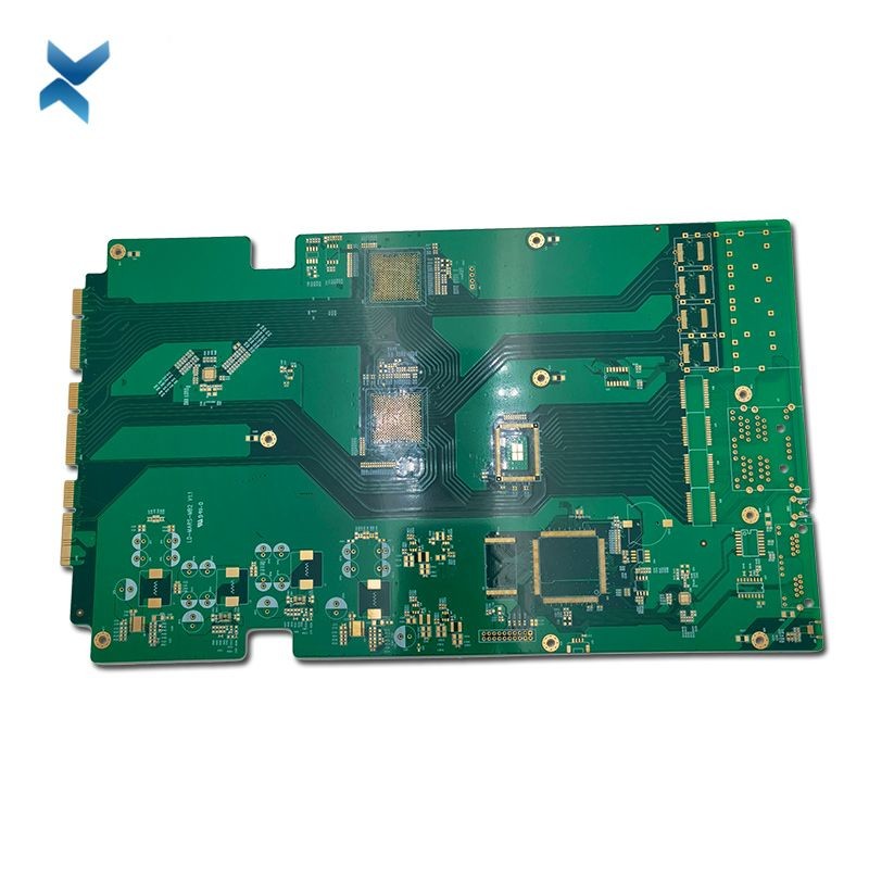
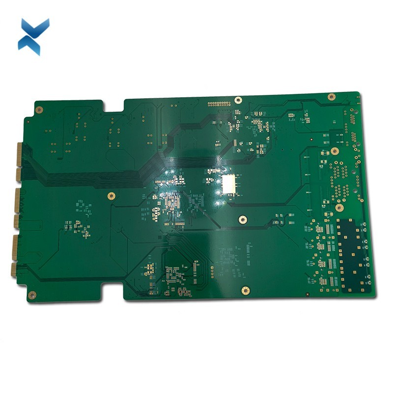
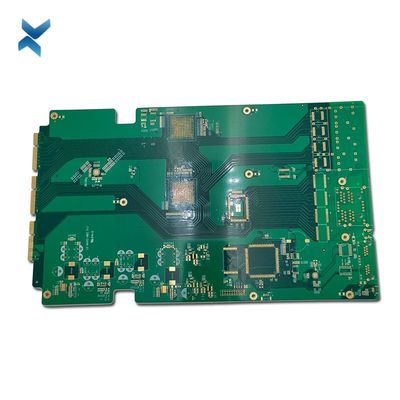
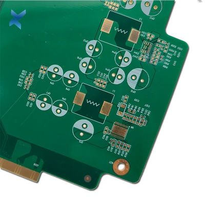
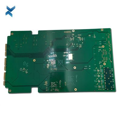
Nickel Plated Atomic Accelerators PCB Circuit Board For Science Experiment
| Place of Origin | Shenzhen |
|---|---|
| Brand Name | YScircuit |
| Certification | ISO9001,UL,REACH, RoHS |
| Model Number | YS-ML-0022 |
| Minimum Order Quantity | 1 |
| Price | $0.04-7/piece |
| Packaging Details | Foam cotton + carton + strap |
| Delivery Time | 2-8 work days |
| Payment Terms | T/T,PayPal, Alibaba pay |
| Supply Ability | 1580000 |

Contact me for free samples and coupons.
Whatsapp:0086 18588475571
Wechat: 0086 18588475571
Skype: sales10@aixton.com
If you have any concern, we provide 24-hour online help.
xProduct Details
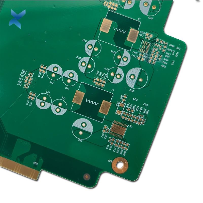
| Product Name | 8 Layer PCB | Surface Finishing | HASL/HASL-LF/ENIG/OSP |
|---|---|---|---|
| Process | Immersion Gold | Copper Thickness | 1.5oz |
| Board Thickness | 1mm | Application | Atomic Accelerators |
| Color | Green | Size | 28*10cm |
| High Light | Nickel Plated PCB Circuit Board,Atomic Accelerators PCB Circuit Board,Atomic Accelerators PCB bare boards |
||
Product Description
Nickel Plated PCB Atomic Accelerators Printed Circuit Boards For Science Experiment
Advantages of Multilayer PCBs over Single Layer Alternatives
When compared to single layer alternatives, the advantages of multilayer PCBs become even more pronounced.
Some of the key improvements multilayer PCBs offer include the following:
• Higher Assembly Density: While single layer PCBs' density is limited by their surface area, multilayer PCBs multiply their density through layering.
This increased density allows greater functionality, improving capacity and speed despite the smaller PCB size.
• Smaller Size: Overall, multilayer PCBs are smaller in size than single layer PCBs.
While single layer PCBs must increase the surface area of the circuit by increasing size, multilayer PCBs increase surface area through the addition of layers, decreasing overall size.
This allows for higher-capacity multilayer PCBs to be used in smaller devices, while high-capacity single layer PCBs must be installed into larger products.
• Lighter Weight: The integration of components in a multilayer PCB means less of a need for connectors and other components, resulting in a lightweight solution for complex electrical applications.
Multilayer PCBs can accomplish the same amount of work as multiple single-layer PCBs, but does so at a smaller size and with fewer connecting components, reducing weight.
This is an essential consideration for smaller electronics where weight is a concern.
• Enhanced Design Functionality: Overall, multilayer PCB bare boards are capable of being more than the average single layer PCB.
With more incorporation of controlled impedance features, greater EMI shielding and overall improved design quality, multilayer PCBs can accomplish more despite their smaller size and lesser weight.
| YS Multilayer PCB manufacturing capabilities overview | ||
| Feature | capabilities | |
| Layer Count | 2-60L | |
| Available Multilayer PCB Technology | Through hole with Aspect Ratio 16:1 | |
| buried and blind via | ||
| Hybrid | High Frequency Material such as RO4350B and FR4 Mix etc. | |
| High Speed Material such as M7NE and FR4 Mix etc. | ||
| Thickness | 0.3mm-8mm | |
| Minimum line Width and Space | 0.05mm/0.05mm(2mil/2mil) | |
| BGA PITCH | 0.35mm | |
| Min mechanical Drilled Size | 0.15mm(6mil) | |
| Aspect Ratio for through hole | 10:1 | |
| Surface Finish | HASL, Lead free HASL,ENIG,Immersion Tin, OSP, Immersion Silver, Gold Finger, Electroplating Hard Gold, Selective OSP,ENEPIG.etc. | |
| Via Fill Option | The via is plated and filled with either conductive or non-conductive epoxy then capped and plated over(VIPPO) | |
| Copper filled, silver filled | ||
| Registration | ±4mil | |
| Solder Mask | Green, Red, Yellow,White, Black, Purple, Matte Black, Matte green.etc. | |
| layer/m² | S<1㎡ | S<3㎡ | S<6㎡ | S<10㎡ | S<13㎡ | S<16㎡ | S<20㎡ | S<30㎡ | S<40㎡ | S<50㎡ | S<65㎡ | S<85㎡ | S<100㎡ |
| 1L | 4wds | 6wds | 7wds | 7wds | 9wds | 9wds | 10wds | 10wds | 10wds | 12wds | 14wds | 15wds | 16wds |
| 2L | 4wds | 6wds | 9wds | 9wds | 11wds | 12wds | 13wds | 13wds | 15wds | 15wds | 15wds | 15wds | 18wds |
| 4L | 6wds | 8wds | 12wds | 12wds | 14wds | 14wds | 14wds | 14wds | 15wds | 20wds | 25wds | 25wds | 28wds |
| 6L | 7wds | 9wds | 13wds | 13wds | 17wds | 18wds | 20wds | 22wds | 24wds | 25wds | 26wds | 28wds | 30wds |
| 8L | 9wds | 12wds | 15wds | 18wds | 20wds | 20wds | 22wds | 24wds | 26wds | 27wds | 28wds | 30wds | 30wds |
| 10L | 10wds | 13wds | 17wds | 18wds | 20wds | 20wds | 22wds | 24wds | 26wds | 27wds | 28wds | 30wds | 30wds |
| 12L | 10wds | 15wds | 17wds | 18wds | 20wds | 20wds | 22wds | 24wds | 26wds | 27wds | 28wds | 30wds | 30wds |
| 14L | 10wds | 16wds | 17wds | 18wds | 20wds | 20wds | 22wds | 24wds | 26wds | 27wds | 28wds | 30wds | 30wds |
| 16L | 10wds | 16wds | 17wds | 18wds | 20wds | 20wds | 22wds | 24wds | 26wds | 27wds | 28wds | 30wds | 30wds |
![]()
![]()
![]()
![]()
![]()
FQA
Q: Do you offer custom layer stack up?
A: We manufacture prototype boards based on default layer stack up. If you need custom layer stack up, please switch to our Standard PCB service. Feel free to request our standard layer stackup at info@ycircuit.com, don't forget to tell us your pcb thickness and layer count.
Q: Can you handle controlled impedance requirements?
A: Yes. Our Standard PCB service offers impedance control option. You may submit the order on PCB Quote page , make a note ""please control impedance within **"" at the Special Requirement Note section. Then submit the order, upload files and release the payment. Your requirement will be known as manufacturing starts.
Q:Can you perform an X-ray inspection after assembly?
A: After assembly, we can launch X-ray test on QFN, LGA, BGA and other components which have bottom pads. Extra cost will be charged for X-ray test.
Recommended Products