


All Products
Contact Person :
Zhou
Phone Number :
+86 15019457904
Whatsapp :
+8615019457904
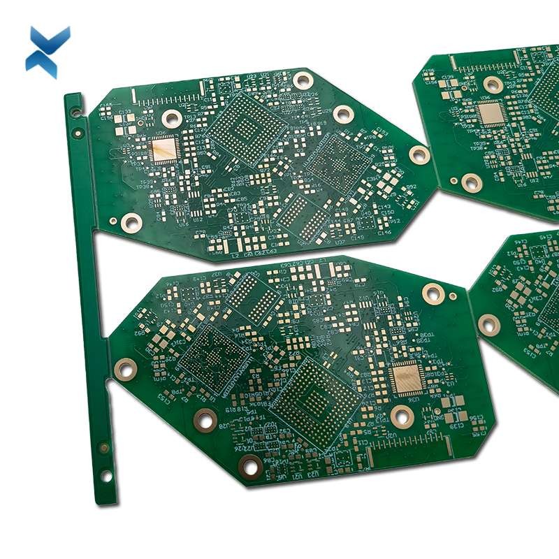
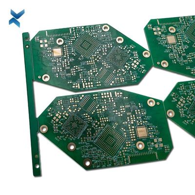
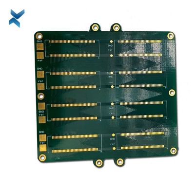
Radio Electronics Multilayer PCB Circuit Board Immersion Gold

Contact me for free samples and coupons.
Whatsapp:0086 18588475571
Wechat: 0086 18588475571
Skype: sales10@aixton.com
If you have any concern, we provide 24-hour online help.
xProduct Details
| Product Name | 2 Layer PCB | Surface Finishing | HASL/HASL-LF/ENIG/OSP |
|---|---|---|---|
| Process | Immersion Gold | Copper Thickness | 1oz |
| Board Thickness | 1.2mm | Application | Radio Machine |
| Color | Dark Green | Size | 8*4cm |
| High Light | Immersion Gold prototype circuit boards,Radio Multilayer PCB Circuit Board,Electronics Multilayer PCB Circuit Board |
||
Product Description
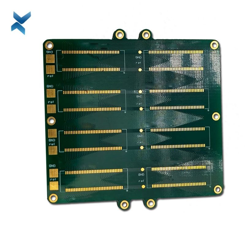
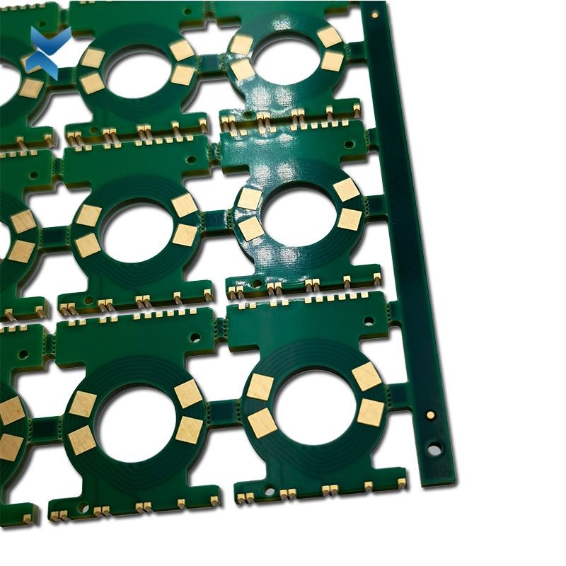
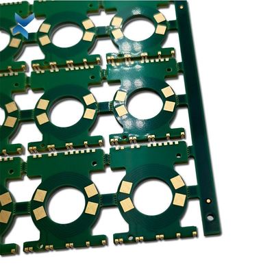
Radio Printed Boards PCB Suitable Electronics Printed Circuit Boards
What is Multilayer PCB?
The multilayer PCB came into being due to the evolving changes in the electronics industry.
The functions of electronics have become progressively more sophisticated over time, requiring more complex PCBs.
Unfortunately, PCBs were limited by problems like noise, stray capacity and crosstalk, and therefore needed to follow certain design constraints.
These design considerations made it difficult to get a satisfactory level of performance from a single or even double-sided PCB - thus the multilayer PCB was born.
Packing the power of a double-layer PCB into a format that's a fraction of the size, multilayer PCBs are becoming increasingly popular in electronics.
They come in a wide range of sizes and thicknesses to accommodate the needs of their expanding applications, with variants ranging anywhere from four to twelve layers.
Layers most often come in even numbers, since odd numbers of layers can cause issues in the circuit like warping, and are no more cost-effective to produce.
Most applications require between four and eight layers, though applications like mobile devices and smartphones tend to use around twelve layers, and some professional PCB manufacturers boast the ability to produce multilayer PCBs with nearly 100 layers.
Multilayer PCBs with that many layers are rare to see, however, as they are extremely cost-inefficient.
prototype circuit boards
| YS Multilayer PCB manufacturing capabilities overview | ||
| Feature | capabilities | |
| Layer Count | 2-60L | |
| Available Multilayer PCB Technology | Through hole with Aspect Ratio 16:1 | |
| buried and blind via | ||
| Hybrid | High Frequency Material such as RO4350B and FR4 Mix etc. | |
| High Speed Material such as M7NE and FR4 Mix etc. | ||
| Thickness | 0.3mm-8mm | |
| Minimum line Width and Space | 0.05mm/0.05mm(2mil/2mil) | |
| BGA PITCH | 0.35mm | |
| Min mechanical Drilled Size | 0.15mm(6mil) | |
| Aspect Ratio for through hole | 10:1 | |
| Surface Finish | HASL, Lead free HASL,ENIG,Immersion Tin, OSP, Immersion Silver, Gold Finger, Electroplating Hard Gold, Selective OSP,ENEPIG.etc. | |
| Via Fill Option | The via is plated and filled with either conductive or non-conductive epoxy then capped and plated over(VIPPO) | |
| Copper filled, silver filled | ||
| Registration | ±4mil | |
| Solder Mask | Green, Red, Yellow,White, Black, Purple, Matte Black, Matte green.etc. | |
| layer/m² | S<1㎡ | S<3㎡ | S<6㎡ | S<10㎡ | S<13㎡ | S<16㎡ | S<20㎡ | S<30㎡ | S<40㎡ | S<50㎡ | S<65㎡ | S<85㎡ | S<100㎡ |
| 1L | 4wds | 6wds | 7wds | 7wds | 9wds | 9wds | 10wds | 10wds | 10wds | 12wds | 14wds | 15wds | 16wds |
| 2L | 4wds | 6wds | 9wds | 9wds | 11wds | 12wds | 13wds | 13wds | 15wds | 15wds | 15wds | 15wds | 18wds |
| 4L | 6wds | 8wds | 12wds | 12wds | 14wds | 14wds | 14wds | 14wds | 15wds | 20wds | 25wds | 25wds | 28wds |
| 6L | 7wds | 9wds | 13wds | 13wds | 17wds | 18wds | 20wds | 22wds | 24wds | 25wds | 26wds | 28wds | 30wds |
| 8L | 9wds | 12wds | 15wds | 18wds | 20wds | 20wds | 22wds | 24wds | 26wds | 27wds | 28wds | 30wds | 30wds |
| 10L | 10wds | 13wds | 17wds | 18wds | 20wds | 20wds | 22wds | 24wds | 26wds | 27wds | 28wds | 30wds | 30wds |
| 12L | 10wds | 15wds | 17wds | 18wds | 20wds | 20wds | 22wds | 24wds | 26wds | 27wds | 28wds | 30wds | 30wds |
| 14L | 10wds | 16wds | 17wds | 18wds | 20wds | 20wds | 22wds | 24wds | 26wds | 27wds | 28wds | 30wds | 30wds |
| 16L | 10wds | 16wds | 17wds | 18wds | 20wds | 20wds | 22wds | 24wds | 26wds | 27wds | 28wds | 30wds | 30wds |
![]()
![]()
![]()
![]()
![]()
FQA
Q: Do you have a UL code?
A: Yes, our UL code is E529345 .
Q: What is the Dielectric Constant of your standard FR4 material?
A: The typical value of our FR4 Tg140 substrate dielectric constant is 4.6, FR4 Tg170 substrate dielectric constant is 4.2.
Q: What is the largest PCB you can make?
A: Prototype PCB: Min 6*6mm | Max 500*500mm
Standard FR4 PCB: Min 6*6mm | Max 600*700mm
Alunimun PCB: Min 6*6mm | Max 610*610mm
Flex PCB: Min 6*6mm, Max 406*610mm
HDI PCB / Flex-rigid pcb / High Frequency PCB / Thick Copper PCB / Halogen-Free PCB: Min 6*6mm | Max 457*610mm
High Tg PCB: Min 6*6mm | Max 500*900mm
Q: What is the largest PCB you can make?
A: Single-sided PCB & Double-sided PCB: Min 150*200 | Max 400*450mm
4-10 layer PCB: Min 203*229 | Max 406*457mm
12-24 layer PCB: Min 305*305 | Max 305*457mm
Q: What is the largest pcb you can make?
A: Max 60*1200mm
Recommended Products