


All Products
Contact Person :
Zhou
Phone Number :
+86 15019457904
Whatsapp :
+8615019457904
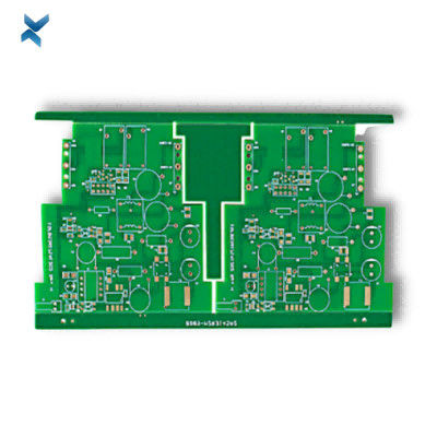
Lead Free HASL 6 Layers Bare Printed Circuit Board For X Ray Equipment


| Place of Origin | Shenzhen |
|---|---|
| Brand Name | YScircuit |
| Certification | ISO9001,UL,REACH, RoHS |
| Model Number | YS-ML-0020 |
| Minimum Order Quantity | 1 |
| Price | $0.04-7/piece |
| Packaging Details | Foam cotton + carton + strap |
| Delivery Time | 2-8 work days |
| Payment Terms | T/T,PayPal, Alibaba pay |
| Supply Ability | 1580000 |

Contact me for free samples and coupons.
Whatsapp:0086 18588475571
Wechat: 0086 18588475571
Skype: sales10@aixton.com
If you have any concern, we provide 24-hour online help.
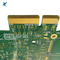
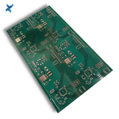
xProduct Details
| Product Name | 6 Layer PCB | Surface Finishing | HASL/HASL-LF/ENIG/OSP |
|---|---|---|---|
| Process | Immersion Gold | Copper Thickness | 1oz |
| Board Thickness | 1.4mm | Application | X-ray Equipment |
| Color | Light Green | Size | 17*5.8cm |
| High Light | HASL Bare Printed Circuit Board,6L Bare Printed Circuit Board,X Ray Equipment PCB |
||
Product Description
Bare Printed Circuit Board 6 Layers Printed Bare Board For X-Ray Equipment
What is Multilayer PCB?
The definition of multilayer PCB is a PCB that is made with three or more conductive copper foil layers.
These appear as several layers of double-sided circuit boards, laminated and glued together with layers of heat-protective insulation between them.
The entire construction is arranged so that two layers are placed on the surface sides of the PCB to connect to the environment.
All electrical connections between the layers are achieved with vias such as plating through holes, blind and buried vias.
Application of this method then leads to the generation of highly complex PCBs of varying sizes.
Multilayer PCB Benefits and Applications
Printed circuit boards (PCBs) are the core of most electronics today, determining basic functions through combinations of components and wiring mechanisms.
Most PCBs of the past were relatively simple and limited by manufacturing techniques, while today's PCBs are much more complex.
From advanced flexible options to odd-shaped varieties, PCBs are much more varied in todays' world of electronics.
While PCBs for simple electronics with limited functions are usually composed of a single layer, more sophisticated electronics, like computer motherboards, consist of multiple layers.
These are what are called multilayer PCBs.
With the increasing complexity of modern electronics, these multilayer PCBs have become more widespread than ever before, while manufacturing techniques have enabled them to size down significantly.
| YS Multilayer PCB manufacturing capabilities overview | ||
| Feature | capabilities | |
| Layer Count | 2-60L | |
| Available Multilayer PCB Technology | Through hole with Aspect Ratio 16:1 | |
| buried and blind via | ||
| Hybrid | High Frequency Material such as RO4350B and FR4 Mix etc. | |
| High Speed Material such as M7NE and FR4 Mix etc. | ||
| Thickness | 0.3mm-8mm | |
| Minimum line Width and Space | 0.05mm/0.05mm(2mil/2mil) | |
| BGA PITCH | 0.35mm | |
| Min mechanical Drilled Size | 0.15mm(6mil) | |
| Aspect Ratio for through hole | 10:1 | |
| Surface Finish | HASL, Lead free HASL,ENIG,Immersion Tin, OSP, Immersion Silver, Gold Finger, Electroplating Hard Gold, Selective OSP,ENEPIG.etc. | |
| Via Fill Option | The via is plated and filled with either conductive or non-conductive epoxy then capped and plated over(VIPPO) | |
| Copper filled, silver filled | ||
| Registration | ±4mil | |
| Solder Mask | Green, Red, Yellow,White, Black, Purple, Matte Black, Matte green.etc. | |
| layer/m² | S<1㎡ | S<3㎡ | S<6㎡ | S<10㎡ | S<13㎡ | S<16㎡ | S<20㎡ | S<30㎡ | S<40㎡ | S<50㎡ | S<65㎡ | S<85㎡ | S<100㎡ |
| 1L | 4wds | 6wds | 7wds | 7wds | 9wds | 9wds | 10wds | 10wds | 10wds | 12wds | 14wds | 15wds | 16wds |
| 2L | 4wds | 6wds | 9wds | 9wds | 11wds | 12wds | 13wds | 13wds | 15wds | 15wds | 15wds | 15wds | 18wds |
| 4L | 6wds | 8wds | 12wds | 12wds | 14wds | 14wds | 14wds | 14wds | 15wds | 20wds | 25wds | 25wds | 28wds |
| 6L | 7wds | 9wds | 13wds | 13wds | 17wds | 18wds | 20wds | 22wds | 24wds | 25wds | 26wds | 28wds | 30wds |
| 8L | 9wds | 12wds | 15wds | 18wds | 20wds | 20wds | 22wds | 24wds | 26wds | 27wds | 28wds | 30wds | 30wds |
| 10L | 10wds | 13wds | 17wds | 18wds | 20wds | 20wds | 22wds | 24wds | 26wds | 27wds | 28wds | 30wds | 30wds |
| 12L | 10wds | 15wds | 17wds | 18wds | 20wds | 20wds | 22wds | 24wds | 26wds | 27wds | 28wds | 30wds | 30wds |
| 14L | 10wds | 16wds | 17wds | 18wds | 20wds | 20wds | 22wds | 24wds | 26wds | 27wds | 28wds | 30wds | 30wds |
| 16L | 10wds | 16wds | 17wds | 18wds | 20wds | 20wds | 22wds | 24wds | 26wds | 27wds | 28wds | 30wds | 30wds |
![]()
![]()
![]()
![]()
![]()
FQA
Q:What does YScircuit do?
A: We're a globally professional provider integrating PCB fabrication, assembly and components sourcing. You can get turnkey PCB services all under one roof.
Q: Do you offer PCB layout or other engineering service?
A: We're capable of taking PCB layout work.
Just send your circuit dirgram / drawing and project requirement to info@yscircuit.com, we will review your demands and quote for engineering and production.
Q: I only have schematic, can you make PCBs for me?
A:Yes. We can do PCB layout based on your schematic, then schedule the production.
Please send your schematic and requirement to info@yscircuit.com, we'll give the quotation accordingly.
Q: Where are your circuit boards manufactured?
A: As a China-based professional PCB manufacturer, all circuit boards are manufactured in China, then ship out to your office.
Q:Do you ship boards to my country?
A: We've shipped PCB boards to customers from over 100 countries in the past 10years and the number keeps rising each year. Surely we can ship boards to your country.
Q: Do you offer free samples?
A: We can offer PCB prototype for you check our quality and delivery time. If you want to verify our quality prior to volume production. Once you've verified our quality, it's easy to repeat the order at any quantity you need.
Recommended Products