


All Products
Contact Person :
Zhou
Phone Number :
+86 15019457904
Whatsapp :
+8615019457904
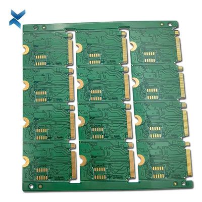
Electronic Multilayer PCB Circuit Board With Immersion Gold Sliver

| Place of Origin | Shenzhen |
|---|---|
| Brand Name | YScircuit |
| Certification | ISO9001,UL,REACH |
| Model Number | YS-ML-0007 |
| Minimum Order Quantity | 1 piece |
| Price | 0.04-5$/piece |
| Packaging Details | Foam cotton + carton + strap |
| Delivery Time | 2-8 days |
| Payment Terms | T/T,PayPal, Alibaba pay, L/C, Western Union, MoneyGram |
| Supply Ability | 251,000 square meter/year |

Contact me for free samples and coupons.
Whatsapp:0086 18588475571
Wechat: 0086 18588475571
Skype: sales10@aixton.com
If you have any concern, we provide 24-hour online help.
xProduct Details
| Material | FR4 | Size | According To Customer Request |
|---|---|---|---|
| Process | Immersion Gold/sliver | Surface Finishing | HASL/HASL-LF/ENIG/OSP |
| Base Material | FR-4 | Min. Line Spacing | 4mil |
| Board Thickness | 1.6mm | Min. Line Width | 3mi |
| High Light | Immersion Gold Multilayer PCB Circuit Board,Immersion Sliver Multilayer PCB Circuit Board,Multilayer electronic circuit board |
||
Product Description
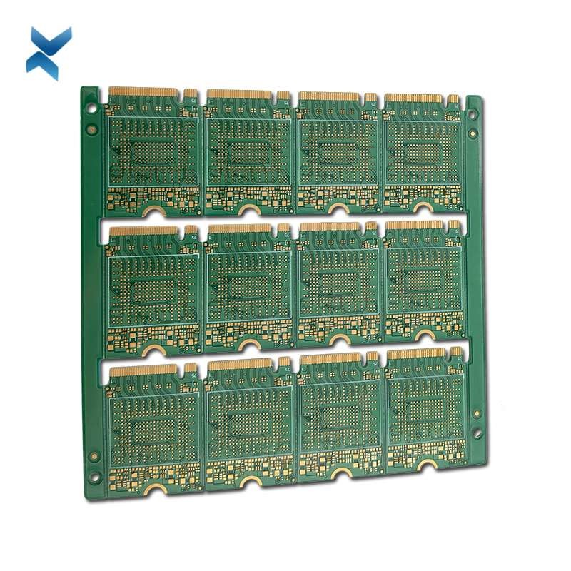
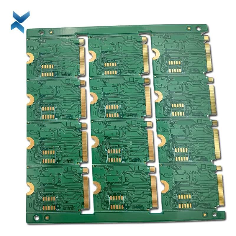
Customized Electronic Circuit Board Turnkey Service Multilayer PCBA Assembly PCB Manufacturer In Shenzhen
What is Multilayer PCBs
Multilayer Printed Circuit Board, It is a type of PCB which comes with a combination of single sided PCB and double sided PCB.
It features layers more than double sided PCB.
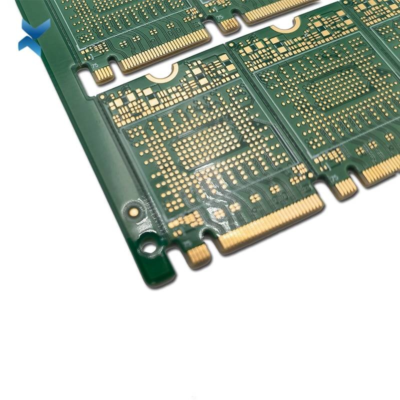
PCB Sideplating
Sideplating is the metalization of the board edge in the PCB filed.
Edge plating, Border plated, plated contour, side metal, these words can also be used to describe the same function.
Half-cut Castellated Holes
Castellations are plated through holes or vias located in the edges of a printed circuit board.
Are indentations created in the form of semi-plated holes on the edges of the PCB boards.
These half holes serve as pads intended to create a link between the module board and the board that it will be soldered onto.
Parameters
- Layers: 6L multilayer pcb
- Board Thinkness:1.0mm
- Base Material:S1000-2 High tg
- Min Holes:0.1mm
- Minimum Line Width/Clearance:0.25mm/0.25mm
- Minimum Clearance between Inner Layer PTH to Line: 0.2mm
- Size:250.6mm×180.5mm
- Aspect Ratio:10 : 1
- Surface treatment:ENIG+ Selective hard gold
- Process characteristics: High tg, Sideplating, Selective hard gold, Half-cut Castellated Holes
- Applications: Wi-Fi modules
| YS Multilayer PCB manufacturing capabilities overview | ||
| Feature | capabilities | |
| Layer Count | 3-60L | |
| Available Multilayer PCB Technology | Through hole with Aspect Ratio 16:1 | |
| buried and blind via | ||
| Hybrid | High Frequency Material such as RO4350B and FR4 Mix etc. | |
| High Speed Material such as M7NE and FR4 Mix etc. | ||
| Thickness | 0.3mm-8mm | |
| Minimum line Width and Space | 0.05mm/0.05mm(2mil/2mil) | |
| BGA PITCH | 0.35mm | |
| Min mechanical Drilled Size | 0.15mm(6mil) | |
| Aspect Ratio for through hole | 16:1 | |
| Surface Finish | HASL, Lead free HASL,ENIG,Immersion Tin, OSP, Immersion Silver, Gold Finger, Electroplating Hard Gold, Selective OSP,ENEPIG.etc. | |
| Via Fill Option | The via is plated and filled with either conductive or non-conductive epoxy then capped and plated over(VIPPO) | |
| Copper filled, silver filled | ||
| Registration | ±4mil | |
| Solder Mask | Green, White, Black, Purple, Matte Black, Matte green.etc. | |
![]()
![]()
![]()
![]()
![]()
FQA
1. What is hard gold in PCB?
The Hard Gold surface finish, also known as Hard Electrolytic Gold, is composed of a layer of gold with added hardeners for increased durability, plated over a barrier coat of nickel using an electrolytic process.
2. What is hard gold plating?
The most common alloying elements used in hard gold plating are cobalt, nickel or iron.
3. What is the difference between Enig and hard gold?
ENIG plating holds up well at only 35 grams of contact force or less, and ENIG plating typically lasts for fewer cycles than hard plating.
A popular trend among manufacturers is board-to-board soldering.
This technique allows companies to produce integrated modules (often containing dozens of parts) on a single board that can be built into another assembly during production.
One easy way to produce a PCB that is destined to be mounted to another PCB is to create castellated mounting holes.
Recommended Products