


All Products
Contact Person :
Zhou
Phone Number :
+86 15019457904
Whatsapp :
+8615019457904
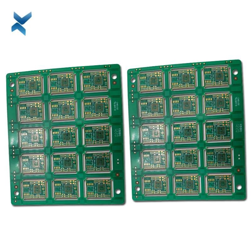
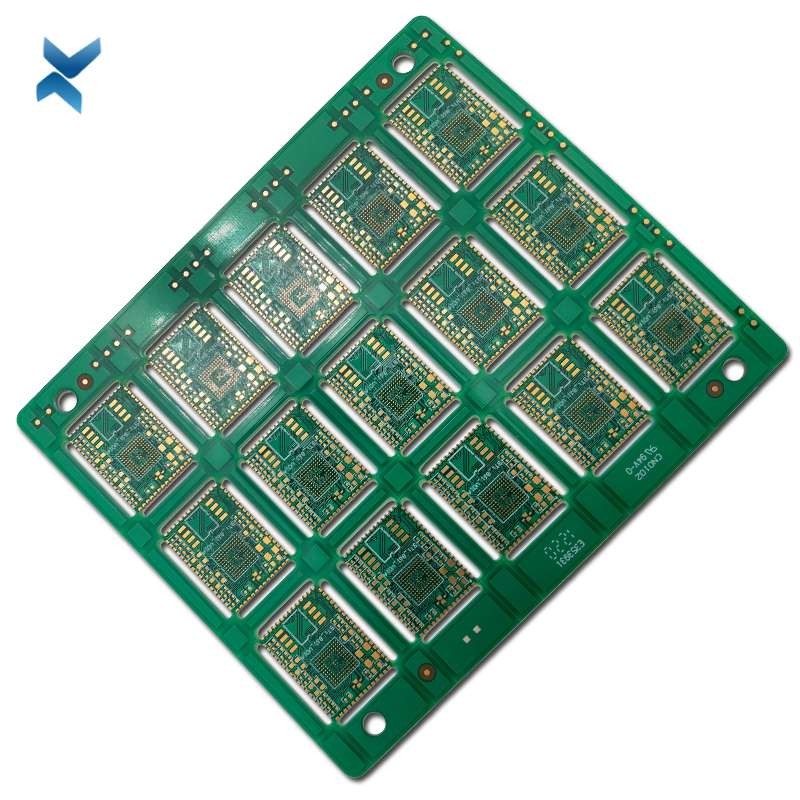
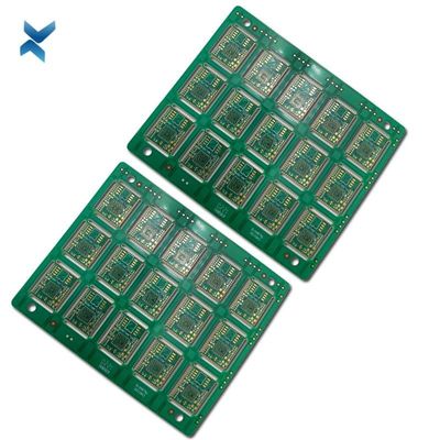
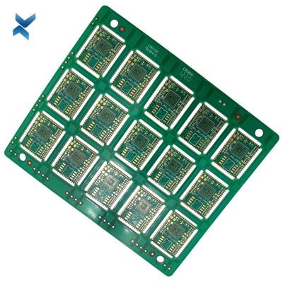
Multilayer PCB Print Circuit Board Assembly With Immersion Gold Sliver Process


| Place of Origin | Shenzhen |
|---|---|
| Brand Name | YScircuit |
| Certification | ISO9001,UL,REACH, RoHS |
| Model Number | YS-ML-0003 |
| Minimum Order Quantity | 1 piece |
| Price | 0.04-5$/piece |
| Packaging Details | Foam cotton + carton + strap |
| Delivery Time | 2-8 days |
| Payment Terms | T/T,PayPal, Alibaba pay |
| Supply Ability | 251,000 square meter/year |

Contact me for free samples and coupons.
Whatsapp:0086 18588475571
Wechat: 0086 18588475571
Skype: sales10@aixton.com
If you have any concern, we provide 24-hour online help.
xProduct Details
| Material | FR4 | Size | According To Customer Request |
|---|---|---|---|
| Process | Immersion Gold/sliver | Surface Finishing | HASL/HASL-LF/ENIG |
| Base Material | FR-4 | Board Thickness | 0.2mm-6mm |
| High Light | Multilayer Print Circuit Board Assembly,Immersion Gold Print Circuit Board Assembly,Immersion Sliver Multilayer PCB Assembly |
||
Product Description
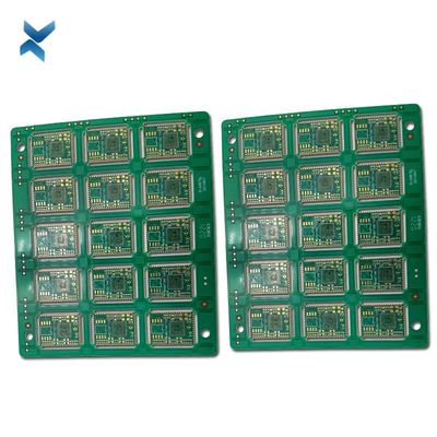
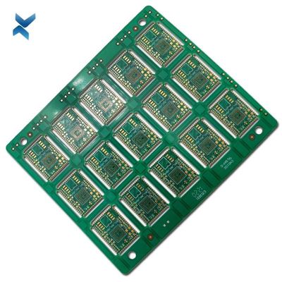
High quality Multilayer PCB assembly print circuit boards Manufacturer in China
What is Multilayer PCBs
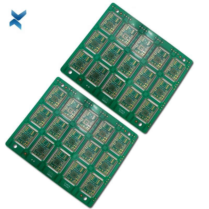
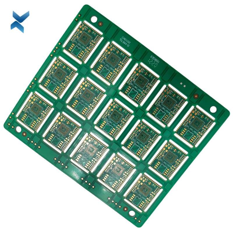
In simple words, Multilayer PCB is a printed circuit board with more than two layers and has a minimum of three conductive layers of conductive material or copper layer. When looking at a multilayer PCB, the top and bottom layers look similar to a double-sided PCB but they have more layers on both sides of the core. These layers are interconnected with copper-plated holes and there can be more layers as we have witnessed up to 40 layers. The active and passive components are placed on the top and bottom layers of the multilayer PCB while the inner stacked layers are used for routing.
How do multilayer PCBs work?
The first step toward the multilayer PCB manufacturing process is to design the layout of the board using any of the PCB designing software, for example, Eagle, Proteus Altium, and KiCAD. Once the design is ready, it is important to make the inner layer core and laminate with desired thickness with copper foil, dry film resist and UV light. The next step in the design workflow is the lamination which includes the inner layer core, prepreg sheets, and copper foil sheets. Next is to apply pressure, heat and vacuum using a heated hydraulic press and it is important to make sure that there is no air trapped between layers. Once cured, resins from the prepregs join the sheets, core and foil to form a multilayer PCB.
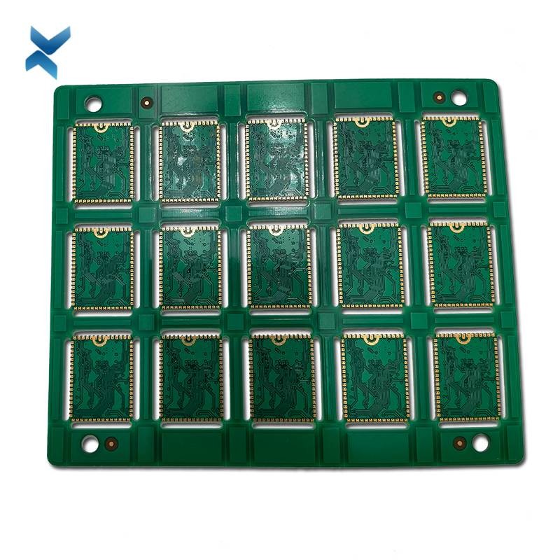
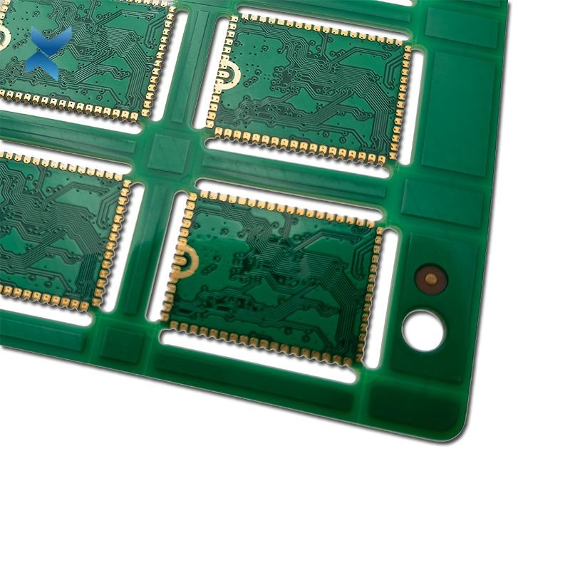
PCB Sideplating
Sideplating is the metalization of the board edge in the PCB filed.
Edge plating, Border plated, plated contour, side metal, these words can also be used to describe the same function.
Half-cut Castellated Holes
Castellations are plated through holes or vias located in the edges of a printed circuit board.
These half holes serve as pads intended to create a link between the module board and the board that it will be soldered onto.
Parameters
- Layers: 8L multilayer pcb
- Board Thinkness:2.0mm
- Base Material:S1000-2 High tg
- Min Holes:0.2mm
- Minimum Line Width/Clearance:0.25mm/0.25mm
- Minimum Clearance between Inner Layer PTH to Line: 0.2mm
- Size:250.6mm×180.5mm
- Aspect Ratio:10 : 1
- Surface treatment:ENIG+ Selective hard gold
- Process characteristics: High tg, Sideplating, Selective hard gold, Half-cut Castellated Holes
- Applications: Wi-Fi modules
| YS Multilayer PCB manufacturing capabilities overview | ||
| Feature | capabilities | |
| Layer Count | 3-60L | |
| Available Multilayer PCB Technology | Through hole with Aspect Ratio 16:1 | |
| buried and blind via | ||
| Hybrid | High Frequency Material such as RO4350B and FR4 Mix etc. | |
| High Speed Material such as M7NE and FR4 Mix etc. | ||
| Thickness | 0.3mm-8mm | |
| Minimum line Width and Space | 0.05mm/0.05mm(2mil/2mil) | |
| BGA PITCH | 0.35mm | |
| Min mechanical Drilled Size | 0.15mm(6mil) | |
| Aspect Ratio for through hole | 16:1 | |
| Surface Finish | HASL, Lead free HASL,ENIG,Immersion Tin, OSP, Immersion Silver, Gold Finger, Electroplating Hard Gold, Selective OSP,ENEPIG.etc. | |
| Via Fill Option | The via is plated and filled with either conductive or non-conductive epoxy then capped and plated over(VIPPO) | |
| Copper filled, silver filled | ||
| Registration | ±4mil | |
| Solder Mask | Green, Red, Yellow, Blue, White, Black, Purple, Matte Black, Matte green.etc. | |
| layer/m² | S<1㎡ | S<3㎡ | S<6㎡ | S<10㎡ | S<13㎡ | S<16㎡ | S<20㎡ | S<30㎡ | S<40㎡ | S<50㎡ | S<65㎡ | S<85㎡ | S<100㎡ |
| 1L | 4wds | 6wds | 7wds | 7wds | 9wds | 9wds | 10wds | 10wds | 10wds | 12wds | 14wds | 15wds | 16wds |
| 2L | 4wds | 6wds | 9wds | 9wds | 11wds | 12wds | 13wds | 13wds | 15wds | 15wds | 15wds | 15wds | 18wds |
| 4L | 6wds | 8wds | 12wds | 12wds | 14wds | 14wds | 14wds | 14wds | 15wds | 20wds | 25wds | 25wds | 28wds |
| 6L | 7wds | 9wds | 13wds | 13wds | 17wds | 18wds | 20wds | 22wds | 24wds | 25wds | 26wds | 28wds | 30wds |
| 8L | 9wds | 12wds | 15wds | 18wds | 20wds | 20wds | 22wds | 24wds | 26wds | 27wds | 28wds | 30wds | 30wds |
| 10L | 10wds | 13wds | 17wds | 18wds | 20wds | 20wds | 22wds | 24wds | 26wds | 27wds | 28wds | 30wds | 30wds |
| 12L | 10wds | 15wds | 17wds | 18wds | 20wds | 20wds | 22wds | 24wds | 26wds | 27wds | 28wds | 30wds | 30wds |
| 14L | 10wds | 16wds | 17wds | 18wds | 20wds | 20wds | 22wds | 24wds | 26wds | 27wds | 28wds | 30wds | 30wds |
| 16L | 10wds | 16wds | 17wds | 18wds | 20wds | 20wds | 22wds | 24wds | 26wds | 27wds | 28wds | 30wds |
|
![]()
![]()
![]()
![]()
![]()
FQA
1. What is hard gold in PCB?
The Hard Gold surface finish, also known as Hard Electrolytic Gold, is composed of a layer of gold with added hardeners for increased durability, plated over a barrier coat of nickel using an electrolytic process.
2. What is hard gold plating?
Hard gold plating is a gold electrodeposit that has been alloyed with another element to alter the grain structure of the gold to achieve a harder deposit with a more refined grain structure.
The most common alloying elements used in hard gold plating are cobalt, nickel or iron.
3. What is the difference between Enig and hard gold?
ENIG plating is much softer than hard gold plating.
Grain sizes are about 60 times larger with ENIG plating, and hardness runs between 20 and 100 HK25.
ENIG plating holds up well at only 35 grams of contact force or less, and ENIG plating typically lasts for fewer cycles than hard plating.
A popular trend among manufacturers is board-to-board soldering.
This technique allows companies to produce integrated modules (often containing dozens of parts) on a single board that can be built into another assembly during production.
One easy way to produce a PCB that is destined to be mounted to another PCB is to create castellated mounting holes.
These are also known as "castellated vias" or "castellations."
Recommended Products