


All Products
Contact Person :
Zhou
Phone Number :
+86 15019457904
Whatsapp :
+8615019457904
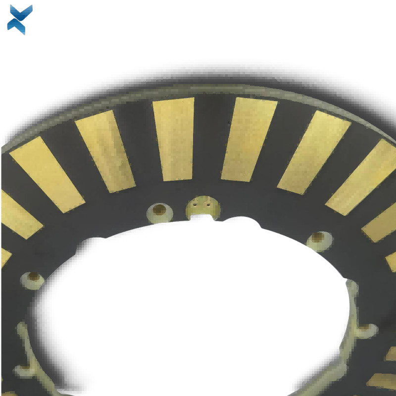
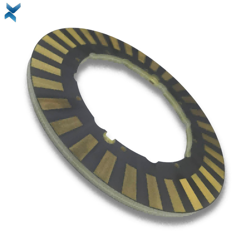
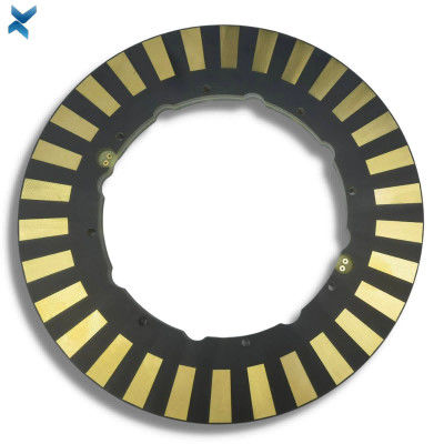
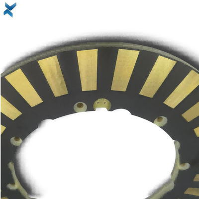
Countersink Pcb Heavy Copper Boards For Medical Machines


| Place of Origin | Shenzhen |
|---|---|
| Brand Name | YScircuit |
| Certification | ISO9001,UL,REACH, RoHS |
| Model Number | YS-HC-0021 |
| Minimum Order Quantity | 1 piece |
| Price | 0.04-5$/piece |
| Packaging Details | Foam cotton + carton + strap |
| Delivery Time | 2-8 days |
| Payment Terms | T/T,PayPal, Alibaba pay |
| Supply Ability | 251,000 square meter/year |

Contact me for free samples and coupons.
Whatsapp:0086 18588475571
Wechat: 0086 18588475571
Skype: sales10@aixton.com
If you have any concern, we provide 24-hour online help.
xProduct Details
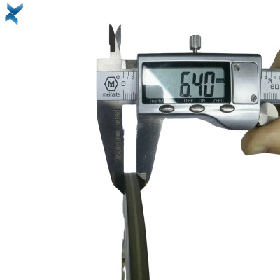
| Material | FR4 | Size | 15*15cm |
|---|---|---|---|
| Process | Immersion Gold | Surface Finishing | ENIG 2u" |
| Layers | 4 Layers | Copper Thickness | 40 Oz |
| Application | Medical Machines | Name | Medical Machines Pcb |
| High Light | Countersink Pcb Heavy Copper Boards,15*15cm Pcb Heavy Copper Boards,FR4 Heavy Copper Pcb Boards |
||
Product Description
Countersink Pcb Heavy Copper Pcb Boards For Medical Machines
What is heavy copper PCB?
Heavy copper PCBs have gained significant popularity across diverse electronic sectors due to societal advancements.
These PCBs offer the capability to incorporate complex switches within confined spaces while ensuring efficient heat dissipation and handling high current levels.
The prevalent designs for heavy copper PCBs include multilayer and double-sided layouts, facilitating the integration of intricate layout structures on the outer layers alongside heavy copper layers within the internal ones.
![]()
The construction of heavy-copper circuits gives the PCBs the following advantages:
1.Increase current capacity greatly
2.Higher endurance to thermal strains
3.Better heat dissipation
4.Increase the mechanical strength at connectors and PTH holes
5.Reduce the product size
| Feature | Capabilities |
| Layer Count | 1-30L |
| Base Material | FR-4 Standard Tg, FR4-mid Tg, FR4-High Tg |
| Thickness | 0.6mm-8.0mm |
| Maximum Outer Layer Copper Weight(Finished) | 15OZ |
| Maximum Inner Layer Copper Weight(Finished) | 30OZ |
| Minimum Line Width and Space | 4OZ Cu 8mil/8mil; 5OZ Cu 10mil; 6OZ Cu 12mil/12mil; 12OZ Cu 18mil/28mil; 15OZ Cu 30mil/38mil.etc. |
| BGA PITCH | 0.8mm(32mil) |
| Min Mechanical Drilled Size | 0.25mm(10mil) |
| Aspect Ratio for Through Hole | 16:1 |
| Surface Finish | HASL, Lead free HASL, ENIG, Immersion Tin, OSP, Immersion Silver, Gold Finger, Electroplating Hard Gold, Selective OSP, ENEPIG.etc. |
| Via Fill Option | The via is plated and filled with either conductive or non-conductive epoxy then capped and plated over(VIPPO) |
| Copper filled, silver filled | |
| Registration | ±4mil |
| Solder Mask | Green, Red, Yellow, Blue, White, Black, Matte Black, Matte Green. etc. |
Along with the increasing of high-power products, the demand for thick-copper PCBs is greatly increased.
Today’s PCB manufacturers pay more attention to using a thick copper board to solve the thermal efficiency of high-power electronics.
The thick-copper PCBs are mostly large current substrate, and large current PCBs are mainly used in power module and automotive electronic parts.
Traditional automotive, power supply, and power electronics applications use the original forms of transmission like cable distribution and metal sheet.
Now the thick-copper boards replace the transmission form, which not only can improve productivity and reduce the time cost of wiring, but also increase the reliability of final products.
At the same time, the massive current boards can improve the design freedom of wiring, thus realizing the miniaturization of the whole product.
Thick-copper circuit PCB play an irreplaceable role in the applications with high-power, high current, and high cooling demand.
The manufacturing process and materials of heavy-copper PCBS have much higher requirements than standard PCBs.
With advanced equipment and professional engineers, YScircuit provides thick-copper PCBs with high-quality for customers from home and abroad.
| layer/m² | S<1㎡ | S<3㎡ | S<6㎡ | S<10㎡ | S<13㎡ | S<16㎡ | S<20㎡ | S<30㎡ | S<40㎡ | S<50㎡ | S<65㎡ | S<85㎡ | S<100㎡ |
| 1L | 4wds | 6wds | 7wds | 7wds | 9wds | 9wds | 10wds | 10wds | 10wds | 12wds | 14wds | 15wds | 16wds |
| 2L | 4wds | 6wds | 9wds | 9wds | 11wds | 12wds | 13wds | 13wds | 15wds | 15wds | 15wds | 15wds | 18wds |
| 4L | 6wds | 8wds | 12wds | 12wds | 14wds | 14wds | 14wds | 14wds | 15wds | 20wds | 25wds | 25wds | 28wds |
| 6L | 7wds | 9wds | 13wds | 13wds | 17wds | 18wds | 20wds | 22wds | 24wds | 25wds | 26wds | 28wds | 30wds |
| 8L | 9wds | 12wds | 15wds | 18wds | 20wds | 20wds | 22wds | 24wds | 26wds | 27wds | 28wds | 30wds | 30wds |
| 10L | 10wds | 13wds | 17wds | 18wds | 20wds | 20wds | 22wds | 24wds | 26wds | 27wds | 28wds | 30wds | 30wds |
| 12L | 10wds | 15wds | 17wds | 18wds | 20wds | 20wds | 22wds | 24wds | 26wds | 27wds | 28wds | 30wds | 30wds |
| 14L | 10wds | 16wds | 17wds | 18wds | 20wds | 20wds | 22wds | 24wds | 26wds | 27wds | 28wds | 30wds | 30wds |
| 16L | 10wds | 16wds | 17wds | 18wds | 20wds | 20wds | 22wds | 24wds | 26wds | 27wds | 28wds | 30wds | 30wds |
Heavy copper pcb stack up
![]() 2OZ-in-inner-layers
2OZ-in-inner-layers
![]() 3OZ-in-inner-layers
3OZ-in-inner-layers
![]() 4L-heavy-copper-PCB-stackup-3oz
4L-heavy-copper-PCB-stackup-3oz
![]()
![]()
![]()
![]()
![]()
FQA
Q: What is a Heavy Copper PCB?
A: A Heavy Copper PCB is a printed circuit board (PCB) with thick copper layers, usually greater than 3 oz per square foot.
Q: What are the benefits of Heavy Copper PCBs?
A: Heavy Copper PCBs have several benefits, including:
- Higher current-carrying capacity
- Improved thermal management
- Increased mechanical strength
- Enhanced reliability and longevity
Q: What applications are Heavy Copper PCBs commonly used in?
A: Heavy Copper PCBs are often used in applications that require high power or high reliability, such as:
Power supplies
Automotive electronics
Industrial equipment
Aerospace and defense electronics
Q: What design considerations should be taken into account when designing Heavy Copper PCBs?
A: When designing Heavy Copper PCBs, it is important to consider:
- The thickness and spacing of copper layers
- The size and placement of vias and through-holes
- The type of substrate material used
- The impact of thermal expansion on the PCB and its components
Q: Can Heavy Copper PCBs be manufactured using standard PCB processes?
A: Yes, Heavy Copper PCBs can be manufactured using standard PCB processes, but special care must be taken to ensure that the thicker copper layers are properly bonded to the substrate and that the PCB is properly plated and etched.
Q: How do I choose the right Heavy Copper PCB manufacturer?
A: When choosing a Heavy Copper PCB manufacturer, consider factors such as:
- Experience and expertise in manufacturing Heavy Copper PCBs
- Quality control processes and certifications
- Production capacity and lead times
- Customer support and communication
Q: What is the cost of Heavy Copper PCBs compared to standard PCBs?
A: Heavy Copper PCBs are generally more expensive than standard PCBs due to the higher cost of materials and the additional manufacturing steps required. However, the benefits of Heavy Copper PCBs may outweigh the higher cost in certain applications.
Recommended Products