


All Products
Contact Person :
Zhou
Phone Number :
+86 15019457904
Whatsapp :
+8615019457904
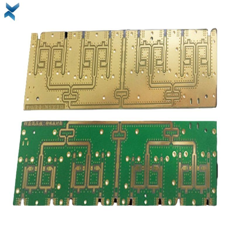
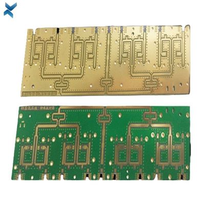
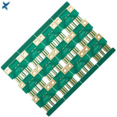
Electronic Circuit Rogers Ro4350B PCB For Aviation Motherboard

| Place of Origin | Shenzhen |
|---|---|
| Brand Name | YScircuit |
| Certification | ISO9001,UL,REACH, RoHS |
| Model Number | Rogers 4350B |
| Minimum Order Quantity | 1 |
| Price | $0.09-6.8/piece |
| Packaging Details | Foam cotton + carton + strap |
| Delivery Time | 2-8 work days |
| Payment Terms | T/T,PayPal, Alibaba pay |
| Supply Ability | 1580000 |

Contact me for free samples and coupons.
Whatsapp:0086 18588475571
Wechat: 0086 18588475571
Skype: sales10@aixton.com
If you have any concern, we provide 24-hour online help.
xProduct Details
| Product Name | ROGERS 4350B PCB | Surface Finishing | ENIG 2u" |
|---|---|---|---|
| Process | Immersion Gold | Copper Thickness | Half Oz |
| Board Thickness | 1.8 Mm | Application | Aviation Motherboard |
| Color | Green | Size | 24*10cm |
| High Light | Electronic Circuit Rogers Ro4350B PCB,Motherboard Rogers Ro4350B PCB,Rogers Ro4350B PCB Electronic Circuit |
||
Product Description
Electronic Circuit Rogers Ro4350B PCB For Aviation Motherboard
Ro4350B PCB Rogers 4350B Material Electronics Boards For Aviation Motherboard
ROGERS 4350B
Achieve precise control over dielectric constant (Dk) with RO4350B laminates, while simultaneously maintaining low loss.
These laminates utilize a standard epoxy/glass processing method, resulting in significant cost savings compared to conventional microwave laminates.
Unlike PTFE-based materials, there is no need for special through-hole treatments or handling procedures.
Additionally, these laminates are UL 94 V-0 rated for active devices and high power RF designs.
Key Features:
Dielectric constant (Dk) of 3.48 with a tolerance of +/- 0.05
Dissipation factor of 0.0037 at 10 GHz
Low Z-axis coefficient of thermal expansion at 32 ppm/°C
Key Benefits:
Fabrication processes similar to FR-4, reducing costs
Competitive pricing in the market
Excellent dimensional stability
|
YS Multilayer PCB manufacturing capabilities overview |
||
|
Feature |
capabilities |
|
|
Layer Count |
2-60L |
|
|
Available Multilayer PCB Technology |
Through hole with Aspect Ratio 16:1 |
|
|
buried and blind via |
||
|
Hybrid |
High Frequency Material such as RO4350B and FR4 Mix etc. |
|
|
High Speed Material such as M7NE and FR4 Mix etc. |
||
|
Thickness |
0.3mm-8mm |
|
|
Minimum line Width and Space |
0.05mm/0.05mm(2mil/2mil) |
|
|
BGA PITCH |
0.35mm |
|
|
Min mechanical Drilled Size |
0.15mm(6mil) |
|
|
Aspect Ratio for through hole |
10:1 |
|
|
Surface Finish |
HASL, Lead free HASL,ENIG,Immersion Tin, OSP, Immersion Silver, Gold Finger, Electroplating Hard Gold, Selective OSP,ENEPIG.etc. |
|
|
Via Fill Option |
The via is plated and filled with either conductive or non-conductive epoxy then capped and plated over(VIPPO) |
|
|
Copper filled, silver filled |
||
|
Registration |
±4mil |
|
|
Solder Mask |
Green, Red, Yellow,White, Black, Purple, Matte Black, Matte green.etc. |
|
|
layer/m² |
S<1㎡ |
S<3㎡ |
S<6㎡ |
S<10㎡ |
S<13㎡ |
S<16㎡ |
S<20㎡ |
S<30㎡ |
S<40㎡ |
S<50㎡ |
S<65㎡ |
S<85㎡ |
S<100㎡ |
|
1L |
4wds |
6wds |
7wds |
7wds |
9wds |
9wds |
10wds |
10wds |
10wds |
12wds |
14wds |
15wds |
16wds |
|
2L |
4wds |
6wds |
9wds |
9wds |
11wds |
12wds |
13wds |
13wds |
15wds |
15wds |
15wds |
15wds |
18wds |
|
4L |
6wds |
8wds |
12wds |
12wds |
14wds |
14wds |
14wds |
14wds |
15wds |
20wds |
25wds |
25wds |
28wds |
|
6L |
7wds |
9wds |
13wds |
13wds |
17wds |
18wds |
20wds |
22wds |
24wds |
25wds |
26wds |
28wds |
30wds |
|
8L |
9wds |
12wds |
15wds |
18wds |
20wds |
20wds |
22wds |
24wds |
26wds |
27wds |
28wds |
30wds |
30wds |
|
10L |
10wds |
13wds |
17wds |
18wds |
20wds |
20wds |
22wds |
24wds |
26wds |
27wds |
28wds |
30wds |
30wds |
|
12L |
10wds |
15wds |
17wds |
18wds |
20wds |
20wds |
22wds |
24wds |
26wds |
27wds |
28wds |
30wds |
30wds |
|
14L |
10wds |
16wds |
17wds |
18wds |
20wds |
20wds |
22wds |
24wds |
26wds |
27wds |
28wds |
30wds |
30wds |
|
16L |
10wds |
16wds |
17wds |
18wds |
20wds |
20wds |
22wds |
24wds |
26wds |
27wds |
28wds |
30wds |
30wds |
![]()
![]()
![]()
![]()
![]()
FQA
What is a Multilayer PCB?
A Multilayer PCB is a printed circuit board that has more than two layers of conductive material separated by insulating layers.
What are the benefits of using a Multilayer PCB?
Multilayer PCBs offer several benefits, such as reduced size and weight, increased functionality, improved performance, and enhanced reliability.
How are Multilayer PCBs manufactured?
Multilayer PCBs are manufactured by layering sheets of conductive material and insulating material together, then laminating and pressing them under heat and pressure.
This process is repeated until the desired number of layers is achieved.
What is the typical number of layers in a Multilayer PCB?
The number of layers in a Multilayer PCB varies depending on the complexity of the circuit design.
Multilayer PCBs can have anywhere from 4 to more than 100 layers.
What is the difference between a Multilayer PCB and a double-sided PCB?
A Multilayer PCB has more than two layers of conductive material separated by insulating layers, while a double-sided PCB has only two layers of conductive material.
What is the maximum number of layers that can be used in a Multilayer PCB?
The maximum number of layers that can be used in a Multilayer PCB is determined by the manufacturing process and the materials used. Typically, Multilayer PCBs have between 4 and 32 layers.
Recommended Products