


All Products
Contact Person :
Zhou
Phone Number :
+86 15019457904
Whatsapp :
+8615019457904
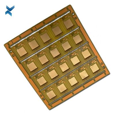
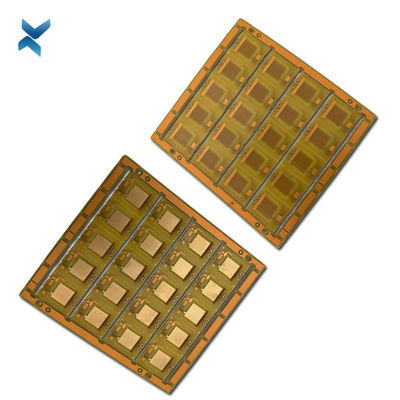
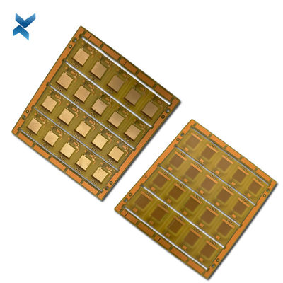
Industrial Electronic Heavy Copper PCB Double Side For Keyboard


| Place of Origin | Shenzhen |
|---|---|
| Brand Name | YScircuit |
| Certification | ISO9001,UL,REACH, RoHS |
| Model Number | YS-HC-0004 |
| Minimum Order Quantity | 1 piece |
| Price | 0.04-5$/piece |
| Packaging Details | Foam cotton + carton + strap |
| Delivery Time | 2-8 days |
| Payment Terms | T/T,PayPal, Alibaba pay |
| Supply Ability | 251,000 square meter/year |

Contact me for free samples and coupons.
Whatsapp:0086 18588475571
Wechat: 0086 18588475571
Skype: sales10@aixton.com
If you have any concern, we provide 24-hour online help.
xProduct Details
| Material | FR4 | Size | According To Customer Request |
|---|---|---|---|
| Process | Immersion Gold/sliver | Surface Finishing | HASL/HASL-LF/ENIG/OSP |
| Layers | Double Side | Thickness | 0.18cm |
| Application | Keyboard | Name | Keyboard Pcb |
| High Light | Electronic Heavy Copper PCB,Industrial Heavy Copper PCB,Keyboard PCB Double Side |
||
Product Description
Double Side Heavy Copper Pcb Print Circuit Bare Boards for Keyboard
Heavy Copper Printed Circuit Boards
Heavy copper printed circuit boards feature 3 ounces of copper in outer/inner layers.
These printed circuit boards are valued immensely, due to their thermal management capabilities.
The heavy copper composition helps keep inner components cool, and improves their performance.
YScircuit provides performance-oriented, heavy copper PCBs, which ensure efficient thermal management and power distribution.
The construction of heavy-copper circuits gives the PCBs the following advantages:
1.Increase current capacity greatly
2.Higher endurance to thermal strains
3.Better heat dissipation
4.Increase the mechanical strength at connectors and PTH holes
5.Reduce the product size
The construction of a heavy copper circuit endows a board with benefits such as:
Increased endurance to thermal strains.
Increased current carrying capacity.
Increased mechanical strength at connector sites and in PTH holes.
Use of exotic materials to their full potential (i.e., high temperature) without circuit failure.
Reduced product size by incorporating multiple copper weights on the same layer of circuitry.
Heavy copper plated vias carry higher current through the board and help to transfer heat to an external heatsink.
On-board heatsinks directly plated onto the board surface using up to 120-oz copper planes.
On-board high-power-density planar transformers
![]()
| Feature | Capabilities |
| Layer Count | 1-30L |
| Base Material | FR-4 Standard Tg, FR4-mid Tg, FR4-High Tg |
| Thickness | 0.6mm-8.0mm |
| Maximum Outer Layer Copper Weight(Finished) | 15OZ |
| Maximum Inner Layer Copper Weight(Finished) | 30OZ |
| Minimum Line Width and Space | 4OZ Cu 8mil/8mil; 5OZ Cu 10mil; 6OZ Cu 12mil/12mil; 12OZ Cu 18mil/28mil; 15OZ Cu 30mil/38mil.etc. |
| BGA PITCH | 0.8mm(32mil) |
| Min Mechanical Drilled Size | 0.25mm(10mil) |
| Aspect Ratio for Through Hole | 16:1 |
| Surface Finish | HASL, Lead free HASL, ENIG, Immersion Tin, OSP, Immersion Silver, Gold Finger, Electroplating Hard Gold, Selective OSP, ENEPIG.etc. |
| Via Fill Option | The via is plated and filled with either conductive or non-conductive epoxy then capped and plated over(VIPPO) |
| Copper filled, silver filled | |
| Registration | ±4mil |
| Solder Mask | Green, Red, Yellow, Blue, White, Black, Matte Black, Matte Green. etc. |
Along with the increasing of high-power products, the demand for thick-copper PCBs is greatly increased.
Today’s PCB manufacturers pay more attention to using a thick copper board to solve the thermal efficiency of high-power electronics.
The thick-copper PCBs are mostly large current substrate, and large current PCBs are mainly used in power module and automotive electronic parts.
Traditional automotive, power supply, and power electronics applications use the original forms of transmission like cable distribution and metal sheet.
Now the thick-copper boards replace the transmission form, which not only can improve productivity and reduce the time cost of wiring, but also increase the reliability of final products.
At the same time, the massive current boards can improve the design freedom of wiring, thus realizing the miniaturization of the whole product.
Thick-copper circuit PCB play an irreplaceable role in the applications with high-power, high current, and high cooling demand.
The manufacturing process and materials of heavy-copper PCBS have much higher requirements than standard PCBs.
With advanced equipment and professional engineers, YScircuit provides thick-copper PCBs with high-quality for customers from home and abroad.
| layer/m² | S<1㎡ | S<3㎡ | S<6㎡ | S<10㎡ | S<13㎡ | S<16㎡ | S<20㎡ | S<30㎡ | S<40㎡ | S<50㎡ | S<65㎡ | S<85㎡ | S<100㎡ |
| 1L | 4wds | 6wds | 7wds | 7wds | 9wds | 9wds | 10wds | 10wds | 10wds | 12wds | 14wds | 15wds | 16wds |
| 2L | 4wds | 6wds | 9wds | 9wds | 11wds | 12wds | 13wds | 13wds | 15wds | 15wds | 15wds | 15wds | 18wds |
| 4L | 6wds | 8wds | 12wds | 12wds | 14wds | 14wds | 14wds | 14wds | 15wds | 20wds | 25wds | 25wds | 28wds |
| 6L | 7wds | 9wds | 13wds | 13wds | 17wds | 18wds | 20wds | 22wds | 24wds | 25wds | 26wds | 28wds | 30wds |
| 8L | 9wds | 12wds | 15wds | 18wds | 20wds | 20wds | 22wds | 24wds | 26wds | 27wds | 28wds | 30wds | 30wds |
| 10L | 10wds | 13wds | 17wds | 18wds | 20wds | 20wds | 22wds | 24wds | 26wds | 27wds | 28wds | 30wds | 30wds |
| 12L | 10wds | 15wds | 17wds | 18wds | 20wds | 20wds | 22wds | 24wds | 26wds | 27wds | 28wds | 30wds | 30wds |
| 14L | 10wds | 16wds | 17wds | 18wds | 20wds | 20wds | 22wds | 24wds | 26wds | 27wds | 28wds | 30wds | 30wds |
| 16L | 10wds | 16wds | 17wds | 18wds | 20wds | 20wds | 22wds | 24wds | 26wds | 27wds | 28wds | 30wds | 30wds |
Heavy copper pcb stack up
![]() 2OZ-in-inner-layers
2OZ-in-inner-layers
![]() 3OZ-in-inner-layers
3OZ-in-inner-layers
![]() 4L-heavy-copper-PCB-stackup-3oz
4L-heavy-copper-PCB-stackup-3oz
| Feature | Capabilities |
| Layer Count | 1-30L |
| Base Material | FR-4 Standard Tg, FR4-mid Tg, FR4-High Tg |
| Thickness | 0.6mm-8.0mm |
| Maximum Outer Layer Copper Weight(Finished) | 15OZ |
| Maximum Inner Layer Copper Weight(Finished) | 30OZ |
| Minimum Line Width and Space | 4OZ Cu 8mil/8mil; 5OZ Cu 10mil; 6OZ Cu 12mil/12mil; 12OZ Cu 18mil/28mil; 15OZ Cu 30mil/38mil.etc. |
| BGA PITCH | 0.8mm(32mil) |
| Min Mechanical Drilled Size | 0.25mm(10mil) |
| Aspect Ratio for Through Hole | 16:1 |
| Surface Finish | HASL, Lead free HASL, ENIG, Immersion Tin, OSP, Immersion Silver, Gold Finger, Electroplating Hard Gold, Selective OSP, ENEPIG.etc. |
| Via Fill Option | The via is plated and filled with either conductive or non-conductive epoxy then capped and plated over(VIPPO) |
| Copper filled, silver filled | |
| Registration | ±4mil |
| Solder Mask | Green, Red, Yellow, Blue, White, Black, Matte Black, Matte Green. etc. |
![]()
![]()
![]()
![]()
![]()
FQA
1. How To Build Heavy Copper PCB?
Standard PCBs are fabricated using standard copper etching and plating processes.
Heavy copper PCBs have a similar construction, but dielectric separation is generally greater with heavier copper. Dielectric separation is the nonconductive substrate between the copper layers.
2. How Much Current Can A Heavy Copper PCB Carry?
How much current can a heavy copper PCB carry?
The answer depends on the amount of heat a printed circuit board can withstand.
In order to determine the maximum current, you must first estimate the heat rise that’s connected to the applied current.
3. Why choose Heavy copper PCBs?
Heavy copper PCBs are essential for applications where a high current flow is required in the circuit.
Without heavy copper traces or lamination, a standard PCB cannot bear the flow of heavy current.
Whenever current flows through a circuit, the electronic components use electrical energy.
There are a large number of heat losses that are commonly known as I2R losses.
Common PCBs cannot take away the heat from the board as heavy copper PCBs do, so the components and the board will become overheated, and due to the failure of components, they stop working on the board.
Thus, a standard PCB cannot deal with the flow of heavy current.
The Power Dissipated can be given as I2R. According to the relation, the magnitude of current highly affects the generated heat.
Heat increases drastically, and it is visible from the square foot power of the current.
We cannot reduce current because of the load, but we still have another factor, which is resistance.
Heavy copper thicknesses traces have a low value of resistance compared to thin traces.
The most important feature of heavy copper PCBs is that they can easily flow heavy currents through them and help in taking the heat away from the board.
There can be heat sinks, and the traces transfer heat to them.
4.How is Heavy Copper PCB Fabricated?
Many PCB manufacturers use different techniques for manufacturing heavy copper PCBs.
Embedded heavy copper method
In this method of fabrication heavy copper PCB by using a flat surface.
Here the heavy copper is added to the prepreg resins.
The thickness of the resin determines the thickness of the copper.
The fabricator positions the laminate into a plating tank for electroplating.
Blue bar method
The blue bar method is done by adding thick copper bars into circuit boards.
This method saves a large amount of material and reduces the weight of the PCB.
During the process of fabrication, the resin flows into space within the copper traces, this helps to achieve an even top surface.
Generally, all the fabricators pay attention to the level of copper fill between inner layers when it comes to multilayer boards with heavy copper layers.
Low levels of fill and low levels of resin can lead to resin hunger.
5. What are the difference between a standard PCB and Thick Copper PCB?
Standard PCBs can also be produced with copper etching and plating processes.
These PCBs are plated to add copper thickness to planes, traces, PTHs, and pads.
The amount of copper used to produce standard PCBs is generally 1oz.
For the production of heavy copper PCB, the amount of copper used is greater than 3oz. For standard circuit boards, copper etching and plating techniques are usually used.
However, heavy copper PCBs are produced by differential etching and step platting.
Standard PCBs perform lighter activities, while heavy copper boards perform multiple heavy duties.
Standard PCBs conduct a low current, while heavy copper PCBs conduct a higher current.
Thick copper PCBs are ideal for high-end applications due to their efficient thermal distribution over the board.
Heavy copper PCBs have better mechanical strength than standard PCBs.
Heavy copper circuit boards enhance the board’s capability in which they are used.
Some other features that make thick copper PCBs different from all other PCBs:
Copper weights:
This is the main distinguishing feature of heavy copper-printed circuit boards.
Copper weights are generally a concern to the weight of the copper used in a square foot area.
This weight is measured in ounces. It shows the actual thickness of the copper layer.
Outer layers:
These are referred to as the finished copper layers of the board.
Electronic components are placed in the external layers.
The external layers begin with copper foil, also coated with copper plating.
This helps to increase the thickness of the board.
The copper weight of the external layers is selected in the initial stages for standard designs.
Heavy copper PCB manufacturers can easily change the weight and thickness of the copper that suits customers’ requirements.
Inner layers:
For any standard project or product, the thickness of the dielectric and the mass of the copper are defined at the initial stages of designing.
While the copper weight and thickness in these layers can be adjusted based on customers’ needs and requirements.
6. How do you choose the thickness of PCB copper?
Many factors determine what thickness of PCB copper you choose.
It would help if you considered the operating temperature, how long it would be exposed to heat, and any chance for a circuit board failure to avoid damage.
7. Why is copper used in PCB?
Copper is the most popular metal for a PCB because it transmits signals effectively and doesn’t lose electricity in the process.
Recommended Products